2 layers50 × 70 mm
Rgbntsc
jamvanderloeff/RGB-to-NTSC
Converts RGB 15kHz video in the form of VGA or SCART into NTSC and/or PAL composite and s-video using
55 parts17MIT

 ldursw/ta7357p4
Functional replacement for the Toshiba TA7357P sync separator IC
Ta7357 is an open-source printed circuit board by ldursw, from the ldursw/ta7357p repository on GitHub, published under the MIT licence. It is a 6-layer board of 23.5 × 8.4 mm with 13 parts on 23 nets, routed with 30 tracks and 32 vias.
It is built around the LM1881, 74HC1G04GW and ME6208A50M3G, with the THS7374 among its other parts. Its parts include 7 capacitors, 4 ICs, 1 resistor and 1 connector.


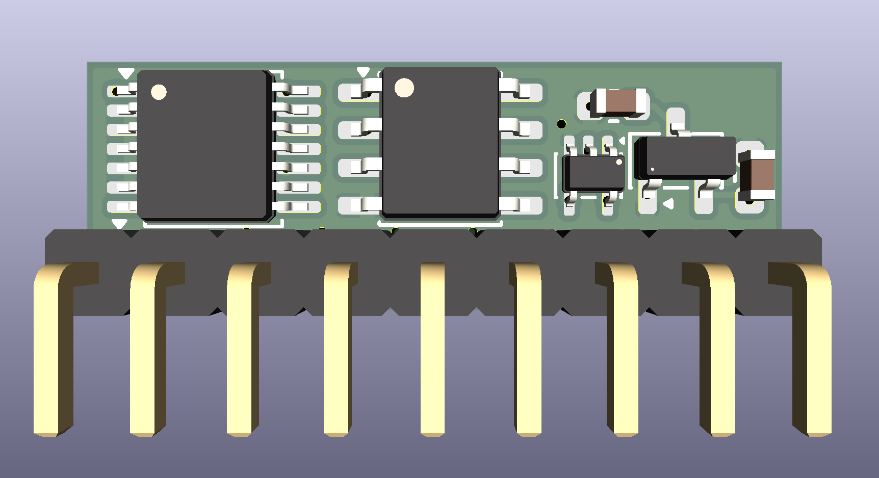
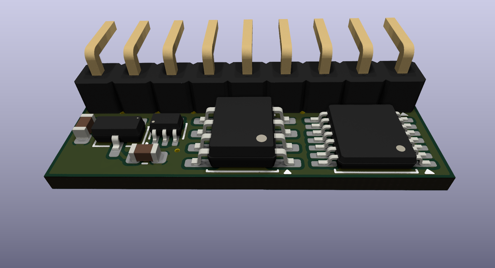
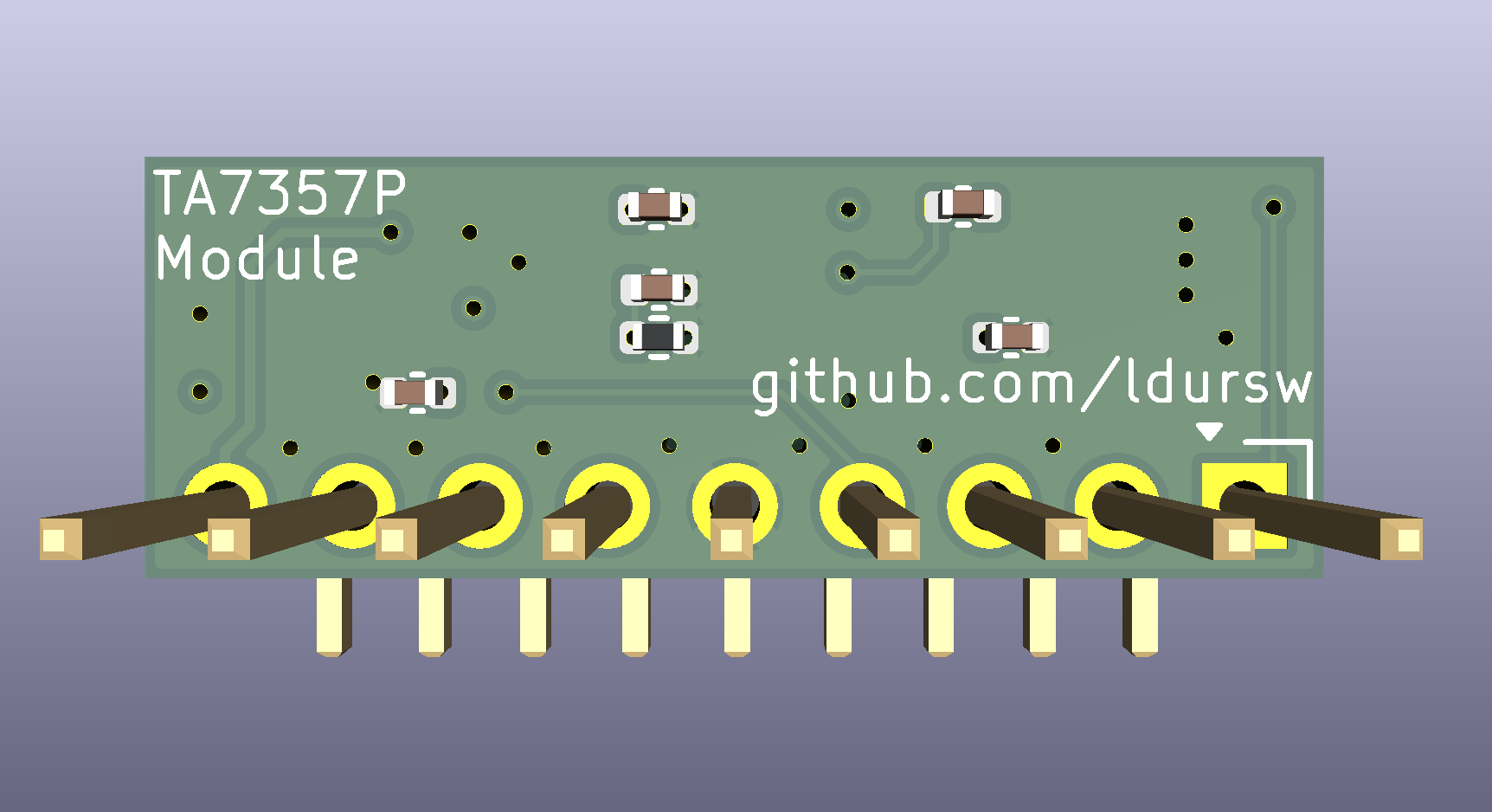
This repository contains a drop-in replacement for the Toshiba TA7357P sync separator IC. This design was successfully used to replace a failed TA7357AP* in a Sony BVW-75 Betacam SP deck.
The board has a 6-layer design and was manufactured by JLCPCB. It is not strictly necessary to be a 6-layer board, but the via-in-pad capability and the low prototype price ($2 for 5 boards) made this a good candidate for testing the resulting PCB quality. Reimplementing this module as a 2-layer board is possible and should work just as well. The circuit is not sensitive and can even be built on a breadboard with the same parts.
The main parts are: THS7374 video amplifier, LM1881 sync separator, 74HC1G04 inverter, and ME6208 5 V regulator.
It is designed to be a drop-in replacement for the original IC, with the same pinout and supply voltage range.
* See the section about the difference between TA7357P and TA7357AP below.
| Side | Back |
|---|---|
 |  |
The original TA7357AP package and functional layout used for this replacement
are included under docs/.
| Original IC | Functional layout |
|---|---|
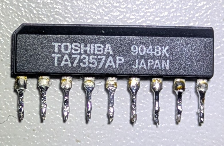 | 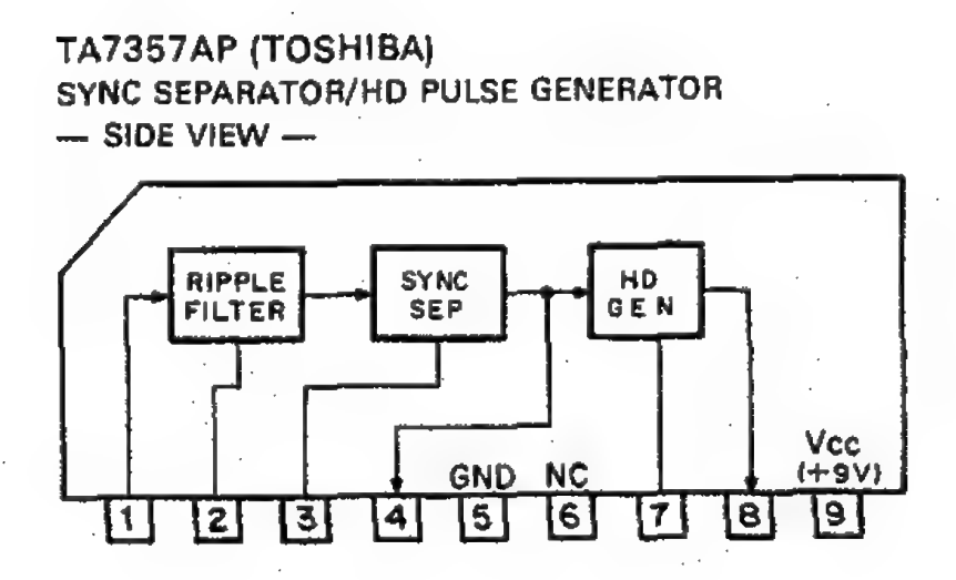 |
The TA7357P is a video sync separator in a 9-pin SIP package. It receives analog video on pin 1 and outputs composite sync on pin 4.
The TA7357AP IC has the same footprint and pinout as the TA7357P, and also has an HD Gen output on pin 8. HD may mean Horizontal Deflection, but this is not confirmed. If the HD Gen output is not used, this module can be used as a replacement for either the TA7357P or TA7357AP.
If you have a Sony BVW-35 deck or other device with a working TA7357AP that uses the HD Gen output and are willing to help, please document the HD Gen output so it can be added to this module in a future revision.
KiCad project files, schematic, PCB layout (for 6 layers), and BOM are included in this repository. The default stack-up was used when ordering the boards from JLCPCB.
Ready-to-order production files are included in the jlcpcb directory and can be used to
order boards from JLCPCB or other PCB manufacturers.
Datasheets and references are included in the docs/ directory.
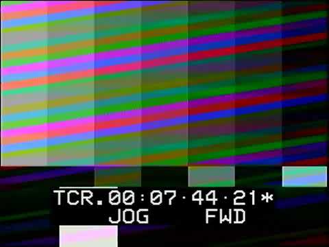
I bought a Sony BVW-75 (Betacam SP broadcast-grade editing VTR) in unknown condition and hoped it would just work or have minor issues. Mechanically it was fine, but it had a major issue in the chroma circuit. The color only showed up if the tape was stopped and Dynamic Tracking (noiseless playback) was turned off. Pressing Play would show diagonal color stripes.
Video demonstrating the issue: https://youtu.be/oWOi9pjKUQA
Based on experience, the artifact looked like a DAC or ADC clock mismatch, so I looked into the machine's TBC, which digitizes the signal to stabilize the video and converts it back to analog for output. After some probing, I noticed the output from a sync separator in the chroma circuit completely disappeared when the gray noise bar wasn't present. My guess was that some internal bias was affecting the threshold for detecting the sync pulses. Without this sync pulse the TBC PLL would lose lock and the memory would not be written or read at the right time.
The sync separator IC has very little information available, so I implemented only the features required for this fix. It would be greatly appreciated if someone could document the HD Gen signal from a working unit that uses it. The IC is completely unobtanium right now, so to fix the machine would require a similar IC. I couldn't find a similar vintage IC in the same package and pinout, so I decided to make a functionally similar module with readily available parts.
My first option was the LM1881, a famous sync separator IC still being manufactured. Looking at the datasheet, I noticed some nuisances: first, there's no package smaller than SOIC-8, which complicates the module design; second, the composite sync output goes low in this IC, whereas the TA7357P goes high, so I would need an inverter as well; third, the supply is 9V, fine for the LM1881 but not for the inverter, so I added a 5V regulator to the mix.
For an experiment, I desoldered the TA7357P, soldered a pin header, and prepared a breadboard with LM1881, LM7805, and 74HC14. Turned everything on and... the picture got worse!?


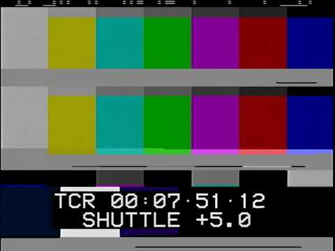
The output from the LM1881 was all over the place, with lots of random pulses that made the PLL even more confused than no pulse at all. I wondered if the input signal wasn't good enough, so I added a THS7374 video amplifier before the sync separator and it worked perfectly on all playback modes.

Video demonstrating the replacement module: https://youtu.be/dzNIqq7tc4I
Then came the PCB layout part. The original IC measures around 22.5 x 5.7 mm and the boards are very close together in the machine, so either I had to make it fit in the same space as the original SIP package or solder wires to the pads and put the replacement board somewhere else.
| Original IC on TBC-7 board | Replacement Module on TBC-7 board |
|---|---|
 |  |
Note: I didn't take a picture of the board before replacing the IC, but through the magic of buying two of them I was able to take a picture after the fact for this post showing before and after the replacement.
Due to the size constraints, I tried to find the smallest package possible that could be hand-soldered. I ended up using a 74HC1G04 inverter in a tiny SOT-353 package, a ME6208A50M3G in a not-so-tiny SOT-23 package, and the THS7374 and LM1881 in huge TSSOP-14 and SOIC-8 packages respectively. The passives are 0402 except for the regulator capacitors which are 0603.
The final module size ended up slightly taller at 23.5 x 8.4 mm, mainly due to the through-hole header footprint. In this specific case it wasn't an issue; there are still a few millimeters of clearance, but that may not be true on an even more cramped machine.
The first board design had 2 layers, but when ordering through JLCPCB I noticed it had the same promotional price for 2- through 8-layer PCBs, so basically more layers for free. 6- and 8-layer boards also have free ENIG finish and via-in-pad. This was an offer I couldn't refuse, so I redid the board layout in 6 layers just so I could use the via-in-pad capability and make the layout cleaner. (Disclaimer: This was not a sponsored project, everything was at my own expense)


The board soldering went smoothly. I tested it on the breadboard first to make sure it worked, and it did on the first try. Then the module got soldered permanently onto the TBC-7 board and a final test confirmed the BVW-75 was fixed.
This project is licensed under the MIT License. See the LICENSE file for details.
| Qty | Value | Footprint | References |
|---|---|---|---|
| 4 | 100n | Capacitor_SMD:C_0402_1005Metric | C1, C2, C3, C7 |
| 2 | 1u | Capacitor_SMD:C_0603_1608Metric | C4, C5 |
| 1 | 47n | Capacitor_SMD:C_0402_1005Metric | C6 |
| 1 | 680K | Resistor_SMD:R_0402_1005Metric | R1 |
| 1 | 74HC1G04 | Package_TO_SOT_SMD:SOT-353_SC-70-5 | U2 |
| 1 | Conn_01x09 | Connector_PinHeader_2.54mm:PinHeader_1x09_P2.54mm_Horizontal | J1 |
| 1 | LM1881 | Package_SO:SOIC-8_3.9x4.9mm_P1.27mm | U1 |
| 1 | ME6208A50M3G | Package_TO_SOT_SMD:SOT-23-3 | U3 |
| 1 | THS7374 | Package_SO:TSSOP-14_4.4x5mm_P0.65mm | U4 |
jamvanderloeff/RGB-to-NTSC
Converts RGB 15kHz video in the form of VGA or SCART into NTSC and/or PAL composite and s-video using


portapack-mayhem/mayhem-firmware
The firmware for the HackRF+PortaPack H1/H2/H4/H4M

jdexyz/SimpleAirQualitySensor
A simple air quality sensor using the Adafruit MagTag e-ink display

Harshad-vali/QWIIC-SWITCH-PROJECT
"Qwiic-compatible I2C power switch module using PCA9536 GPIO expander — KiCad schematic, PCB layout, and BOM."

xenbedded/pixel-c-support
Support hardware and software for running custom code on the Google Pixel C.

It measures 23.5 × 8.4 mm and has 6 copper layers, 1.17 mm thick.
13 parts, built around the LM1881, 74HC1G04GW, ME6208A50M3G and THS7374. The full list of its parts is on this page, with links to each part's symbol and footprint where PCBKit's library has them.
From the ldursw/ta7357p repository on GitHub, at the commit this page was made from: the board is ta7357.kicad_pcb and its schematic ta7357.kicad_sch. PCBKit opens the board in the browser, with nothing to install.
Its repository publishes it under the MIT licence: you may reuse it on that licence's terms (keep the author's notice, and for a copyleft licence share your changes alike).