

2 layers78.7 × 58.4 mm

 jiroegbu-eng/Solar_USB_Buck_Converter
KiCad PCB design for a 12–20V solar-input to 5V USB buck converter using LM2596S-ADJ.
Solar USB Buck Converter is an open-source printed circuit board by jiroegbu-eng, from the jiroegbu-eng/Solar_USB_Buck_Converter repository on GitHub. It is a 2-layer board of 99.9 × 46.5 mm with 11 parts on 7 nets, routed with 75 tracks and 0 vias.
It is built around the LM2596S-ADJ and SS34. Its parts include 4 capacitors, 2 resistors, 2 connectors, 1 IC and 1 diode. It belongs with the power boards of this library.
This project is a KiCad PCB design for a solar-powered buck converter that steps down a 12–20V DC solar input to a 5V USB output. The goal was to design a compact power board that could support off-grid IoT devices, sensor nodes, and small embedded electronics.
The project was built as part of my EDA portfolio to practice switch-mode power supply layout, component placement, PCB routing, ground pours, and clean design-rule validation.
Many field-deployed IoT systems need a simple and reliable way to generate 5V from a small solar panel. This board explores that idea using a practical LM2596-based buck converter design.
The portfolio angle for this project is simple:
Built for Africa's off-grid reality — a compact solar-to-USB power stage for IoT sensor nodes and field-deployed electronics.
| Parameter | Value |
|---|---|
| Input Voltage | 12–20V DC |
| Output Voltage | 5V USB |
| Regulator | LM2596S-ADJ |
| Output Connector | USB Type-A |
| Input Connector | 2-pin screw terminal |
| Inductor | 100µH |
| Freewheel Diode | SS34 Schottky diode |
| Bulk Capacitors | 220µF input/output |
| Decoupling Capacitors | 100nF ceramic |
| PCB Tool | KiCad |
| Status | Schematic and PCB complete |
The circuit takes a 12–20V solar panel input and feeds it into an LM2596 adjustable buck regulator. The regulator drives a switching node connected to a Schottky diode and 100µH inductor. The output is filtered with a 220µF bulk capacitor and a 100nF ceramic capacitor before feeding the USB 5V output.
The feedback divider uses 1kΩ and 3.1kΩ resistors to set the output close to 5V.
Approximate output voltage:
Vout = 1.23 × (1 + 3.1k / 1k)
Vout ≈ 5.04VThe PCB layout was designed with switch-mode power supply layout practices in mind:
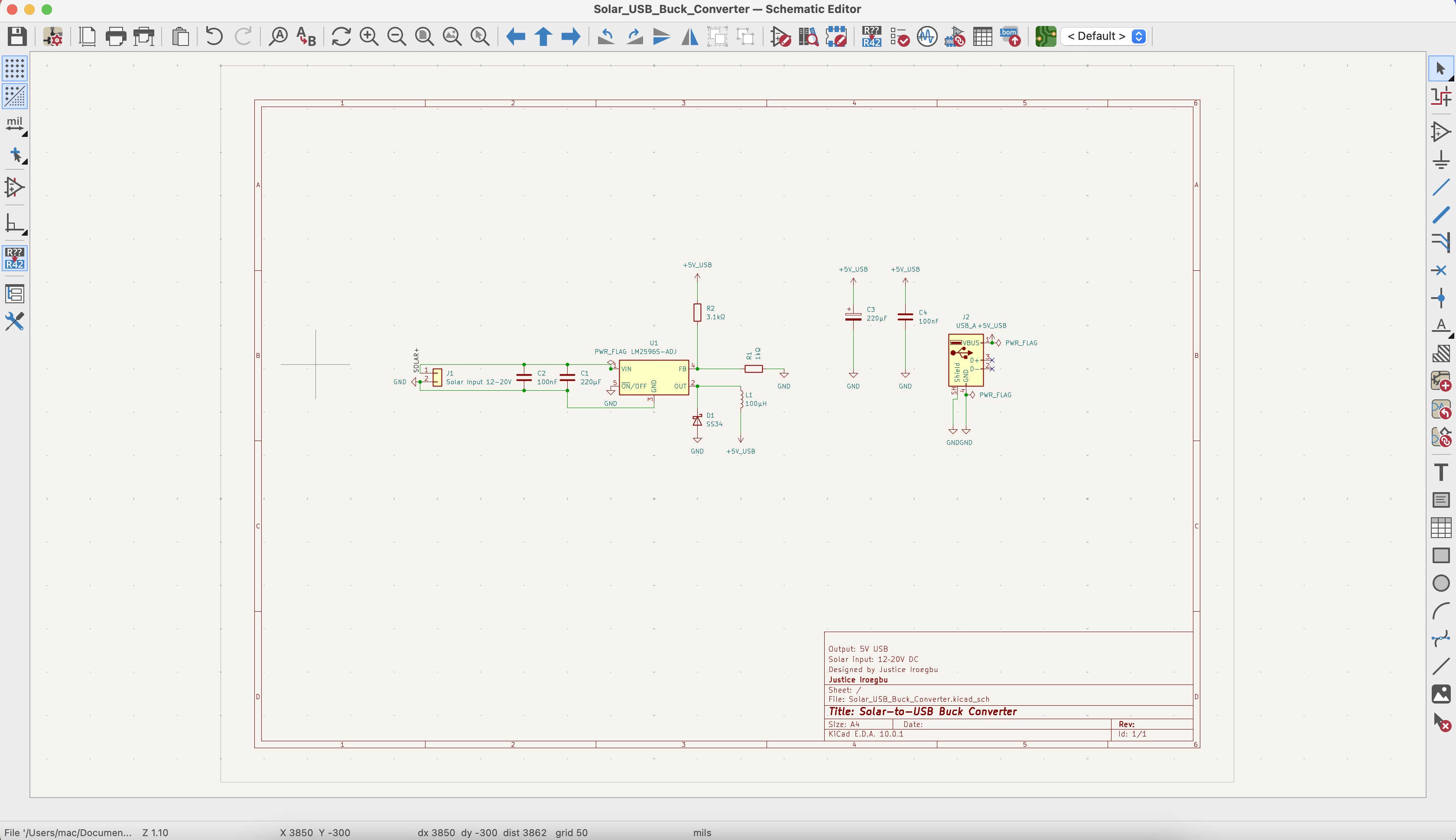
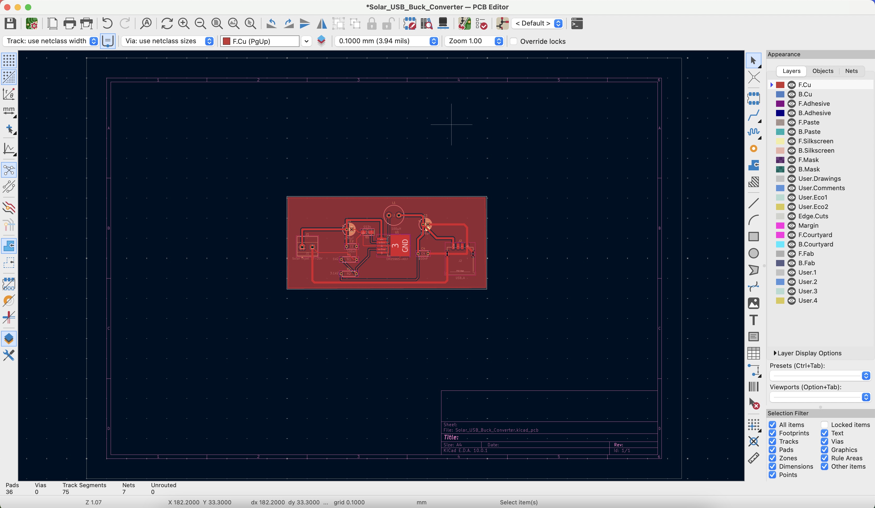
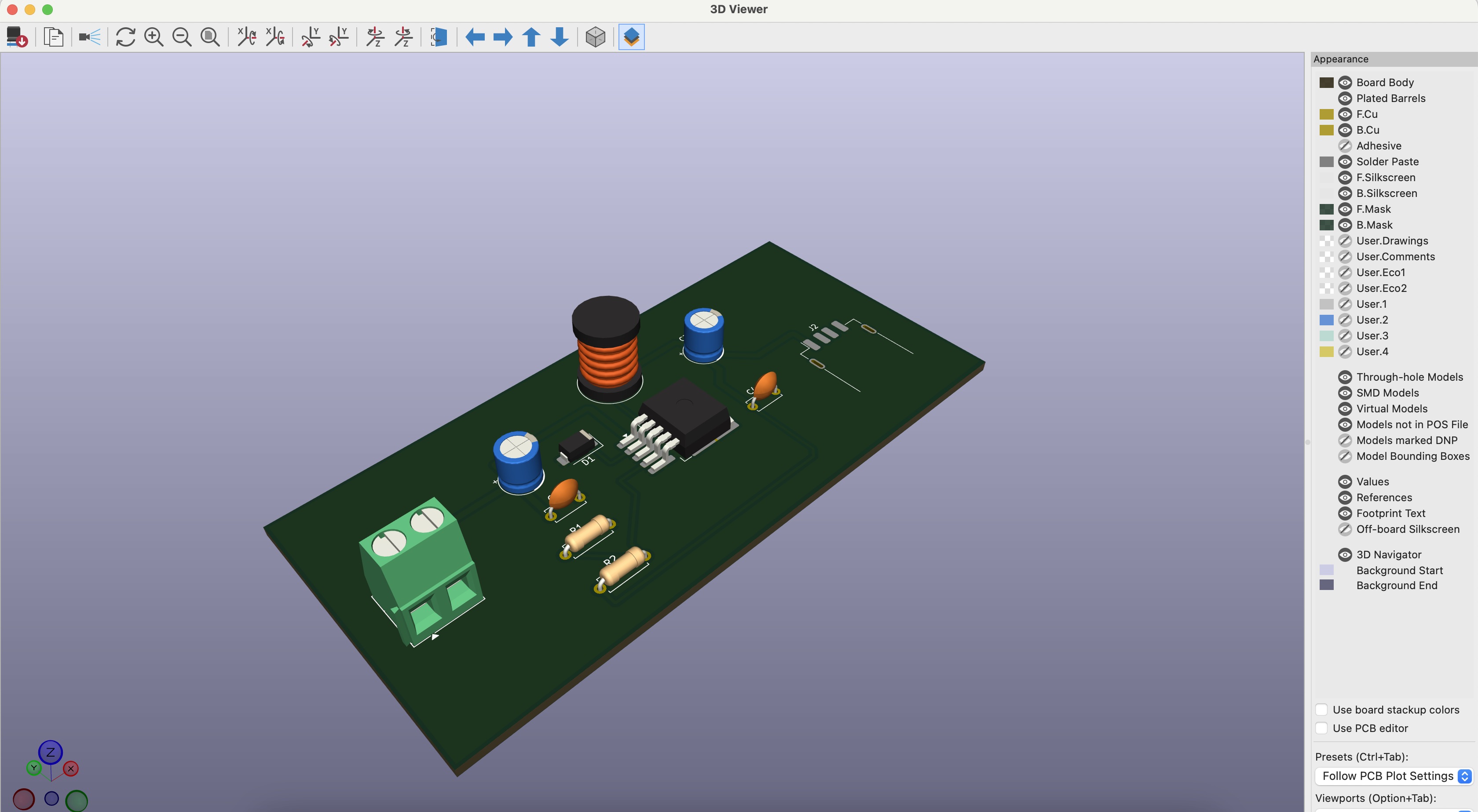
| File | Description |
|---|---|
Solar_USB_Buck_Converter.kicad_pro | KiCad project file |
Solar_USB_Buck_Converter.kicad_sch | Circuit schematic |
Solar_USB_Buck_Converter.kicad_pcb | PCB layout |
Solar_USB_Buck_Converter.kicad_prl | KiCad project local settings |
images/ | Project screenshots |
Completed:
Planned future improvements:
This project helped me understand the practical layout concerns of switch-mode power supplies. The biggest lesson was that buck converters are not just about connecting the right components; placement and routing matter a lot. The switching loop, diode placement, inductor position, capacitor location, and ground return paths all affect how clean and reliable the design can be.
It also helped me get more comfortable moving from schematic capture to PCB layout, assigning footprints, routing power traces, adding copper pours, checking DRC results, and generating a 3D board preview.
| Qty | Value | Footprint | References |
|---|---|---|---|
| 2 | 100nF | Capacitor_THT:C_Disc_D5.0mm_W2.5mm_P5.00mm | C2, C4 |
| 2 | 220µF | Capacitor_THT:CP_Radial_D6.3mm_P2.50mm | C1, C3 |
| 1 | 100µH | Inductor_THT:L_Radial_D10.0mm_P5.00mm_Fastron_07M | L1 |
| 1 | 1kΩ | Resistor_THT:R_Axial_DIN0207_L6.3mm_D2.5mm_P7.62mm_Horizontal | R1 |
| 1 | 3.1kΩ | Resistor_THT:R_Axial_DIN0207_L6.3mm_D2.5mm_P7.62mm_Horizontal | R2 |
| 1 | LM2596S-ADJ | Package_TO_SOT_SMD:TO-263-5_TabPin3 | U1 |
| 1 | SS34 | Diode_SMD:D_SMA | D1 |
| 1 | Solar Input 12-20V | TerminalBlock_Phoenix:TerminalBlock_Phoenix_MKDS-1,5-2-5.08_1x02_P5.08mm_Horizontal | J1 |
| 1 | USB_A | Connector_USB:USB_A_Receptacle_GCT_USB1046 | J2 |

Aleksei327/ESP32-C5-OBD2-Scanner
DIY dual-CAN OBD2 adapter on Seeed XIAO ESP32-C5 with a Flutter Android app. Working prototype, tested on a Citroën C3 II: full read-only ECU scan, PSA fault codes, live data. Single-sided home-etched KiCad board.

0BitsnBytes/McQueen
an overpowered rc car that poses a danger to my safety :)


ZonatedCord/Yggdrasill
Smart LED plant pot — ESP32 PCB, WS2812B/SK6812 LEDs, WLED firmware, modular 3D-printed vase, and a native iOS app with Apple's Liquid Glass design.

IKGB105/LM2596-Adjustable-Buck-Converter
Adjustable LM2596 buck converter — KiCad PCB + COMSOL thermal validation, documented as an honest engineering logbook

ilomon10/embedded-totalizer-hour-meter
ESP32 engine hour meter & totalizer: firmware, SensorFrame protocol, Node host tools, KiCad PCB and a Deno device simulator

It measures 99.9 × 46.5 mm and has 2 copper layers, 1.6 mm thick.
11 parts, built around the LM2596S-ADJ and SS34. The full list of its parts is on this page, with links to each part's symbol and footprint where PCBKit's library has them.
From the jiroegbu-eng/Solar_USB_Buck_Converter repository on GitHub, at the commit this page was made from: the board is Solar_USB_Buck_Converter.kicad_pcb and its schematic Solar_USB_Buck_Converter.kicad_sch. PCBKit opens the board in the browser, with nothing to install.
Its repository states no licence, so its author keeps all rights: ask jiroegbu-eng before reusing the design.