DIY dual-CAN OBD2 adapter on Seeed XIAO ESP32-C5 with a Flutter Android app. Working prototype, tested on a Citroën C3 II: full read-only ECU scan, PSA fault codes, live data. Single-sided home-etched KiCad board. Docs in English and Russian.
Scaner v1 is an open-source printed circuit board by Aleksei327, from the Aleksei327/ESP32-C5-OBD2-Scanner repository on GitHub. It is a 2-layer board of 40 × 60 mm with 34 parts on 25 nets, routed with 228 tracks and 0 vias.
It is built around the SN65HVD230D, LM2596S-ADJ and SS34, with the 1.5KE6.8CA, HS1M and IRFB4110 among its other parts. Its parts include 10 resistors, 8 capacitors, 6 diodes, 4 ICs and 2 connectors. It belongs with the interfaces and adapters boards and the ESP32 and RISC-V boards of this library.
KiCad 10 project of the adapter board: 40 × 60 mm, single-sided (all tracks on the bottom copper, no wire jumpers), designed for home etching and built into an OBD2 enclosure. Description and design notes: DOCS/en/board-v1.md.
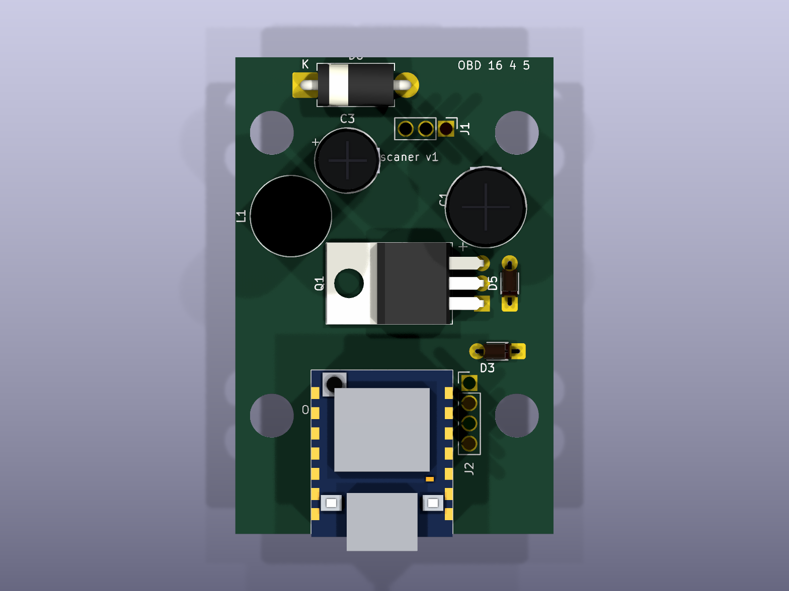
Top
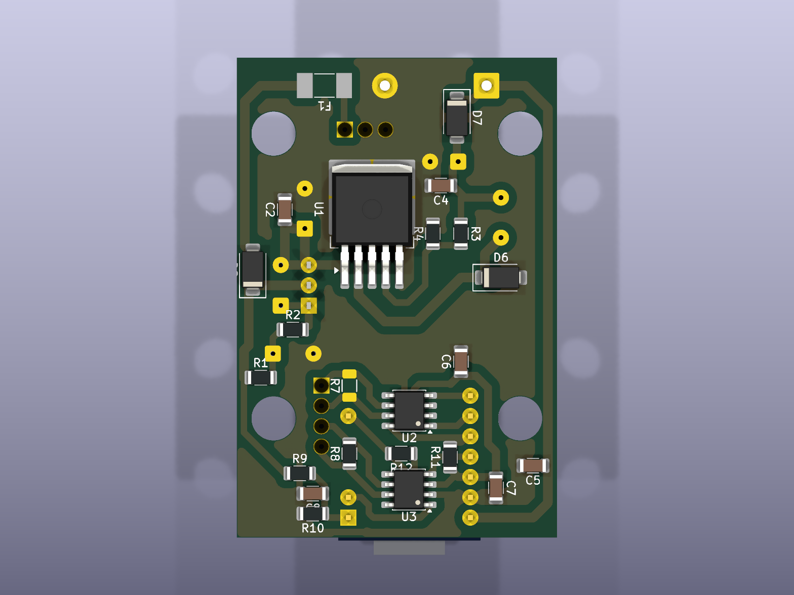
Bottom
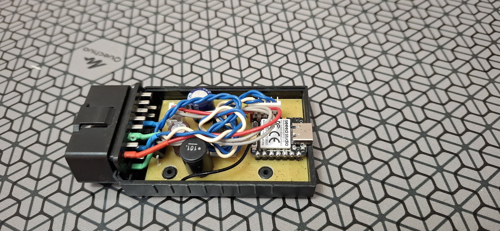
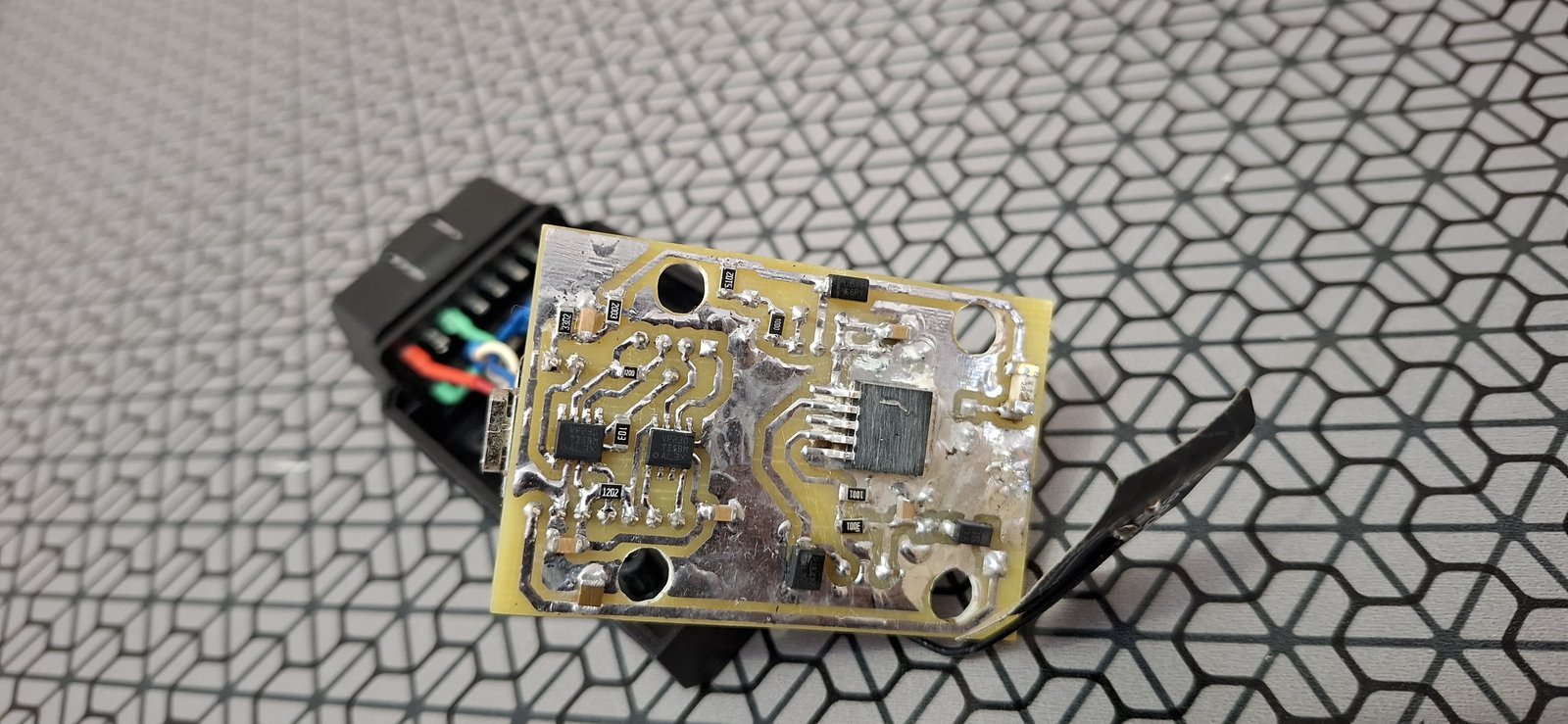
Top row: KiCad 3D. Bottom row: the board as built, in its enclosure and from the copper side.
schematic, board, project (design rules: 0.8 mm tracks, 0.4 mm clearance)
scaner.pretty/
project footprints: XIAO ESP32-C5 on two 1×7 sockets, DO-35 zener at 5.08 mm pitch, OBD2 enclosure outline
scaner.3dshapes/
hand-written 3D models (VRML) for parts missing from the KiCad library
build/*.pdf
schematic, placement with copper, bottom copper 1:1 for etching
tools/
Python scripts that generate everything (see below)
The board is generated, not drawn by hand
The schematic, placement and routing are produced by scripts, so a change is made in the script and everything is regenerated:
sh
python tools/gen_schematic.py # parts, nets, project footprints -> scaner_v1.kicad_sch
python tools/check_netlist.py # ERC and netlist check against tools/expected_nets.json"C:\Program Files\KiCad\10.0\bin\python.exe" tools/gen_pcb.py # placement (PLACE table), pad rules, keep-outs"C:\Program Files\KiCad\10.0\bin\python.exe" tools/hand_route.py # tracks from tools/routes.py, ground pour, DRC
python tools/gen_3d.py # 3D models into scaner.3dshapes/
routes.py — every track as a list of points (or REF.pad references) with its width.
view_board.py — an SVG view of the board with net names on the pads, ratsnest and DRC markers; handy while routing.
route.py — Freerouting experiment kept for reference; it overwrites the hand routing.
Manual edits made in KiCad are overwritten by the next gen_pcb.py / hand_route.py run — carry them over into routes.py first.
The 40 × 60 mm board for the enclosure was placed and routed by hand in KiCad (October 2026), then etched and assembled. Do not run gen_pcb.py or hand_route.py: they bring back the old 40 × 70 board and overwrite the manual work; routes.py is the old routing, kept for reference. Values in the schematic and on the board match what is soldered: R1 51k, R9 200k, R11 12k, R8 fitted, R7 left out.
Printing for etching
KiCad's Print dialog is awkward for photoresist work, so there is a print window of its own — the
"Печать для травления" button in the PCB editor (or tools/etch_window.cmd without KiCad):
sh
"C:\Program Files\KiCad\10.0\bin\python.exe" tools/etch_window.py --pack # tools/etch_print_kicad_plugin.zip for KiCad's Plugin and Content Manager"C:\Program Files\KiCad\10.0\bin\python.exe" tools/etch_window.py --install # while editing the code: button loaded straight from the repo (silent if the package is installed)"C:\Program Files\KiCad\10.0\bin\python.exe" tools/etch_print.py # no window: 4 PDFs in etch/ with an automatic layout
To get the button: KiCad → Plugin and Content Manager → Install from File… → tools/etch_print_kicad_plugin.zip.
The package lives in Documents\KiCad\<version>\3rdparty and survives a KiCad reinstall; after a new KiCad
version install the zip again. After changing the code, run --pack and reinstall the package.
Settings on the left (scrollable), the sheet on the right; drag the divider between them.
An A4 sheet like a print preview: drag board copies with the mouse (arrow keys move 0.5 mm), "+ copy",
"fill the sheet"; a red frame marks copies that overlap or leave the printer's printable area.
Negative (dry-film resist: clear = copper stays) or positive (toner transfer); "toner down / up" sets the
mirroring: the bottom layer laid toner-to-copper prints unmirrored (KiCad shows it from the top, through the board).
Prints straight to the printer at 1:1, no PDF viewer involved. "Film: maximum" stores a printer profile with
the transparency media type, best quality and toner saving off; "Driver settings…" stores any driver settings
(%APPDATA%\etch_print). Toner density on the HP M1530 is set in the printer's own menu.
On the sheet: 100 mm rulers on both axes to check the scale, drill dots, crosses at mounting-hole centres,
corner marks at the board edges. Zones are refilled before printing; the layout is kept in etch/layout.json.
Enclosure
The OBD2 enclosure (72 × 46 × 26, AliExpress) is modelled from measurements by a FreeCAD script:
sh
"C:\Program Files\FreeCAD 1.0\bin\python.exe" tools/gen_case.py # model, drawings, enclosure layer for KiCad"C:\Program Files\KiCad\10.0\bin\python.exe" tools/render_case.py # pictures of the enclosure and the board inside
case/*.step, case/case.FCStd — 3D model for FreeCAD and other tools.
scaner.pretty/Case_OBD2_72x46 — a board-only, locked "enclosure" footprint (CASE1): the "Корпус внутри" layer
(Eco1) shows walls, posts, plug pins and heights; "Корпус снаружи" (Eco2) the outside; a dashed outline on
User.Drawings marks the 40 × 60 board. In the 3D viewer the enclosure is translucent, board bottom 5 mm above the floor.
Precision 0–50 V programmable laboratory PSU with 1 mV/1 mA setting steps, hybrid synchronous-buck + linear regulation, STM32G474 control, INA228 metering, and layered hardware protection.
an overpowered rc car that poses a danger to my safety :)
192 parts1GPL-3.0
Questions
How big is the Scaner v1 PCB?
It measures 40 × 60 mm and has 2 copper layers, 1.6 mm thick.
What parts does the Scaner v1 use?
34 parts, built around the SN65HVD230D, LM2596S-ADJ, SS34 and 1.5KE6.8CA. The full list of its parts is on this page, with links to each part's symbol and footprint where PCBKit's library has them.
Where can I download the Scaner v1 KiCad files?
From the Aleksei327/ESP32-C5-OBD2-Scanner repository on GitHub, at the commit this page was made from: the board is hardware/scaner_v1/scaner_v1.kicad_pcb and its schematic hardware/scaner_v1/scaner_v1.kicad_sch. PCBKit opens the board in the browser, with nothing to install.
Can I use the Scaner v1 design in my own project?
Its repository states no licence, so its author keeps all rights: ask Aleksei327 before reusing the design.