
2 layers354.5 × 132.5 mm
Panels001
jibonaronno/documentsA
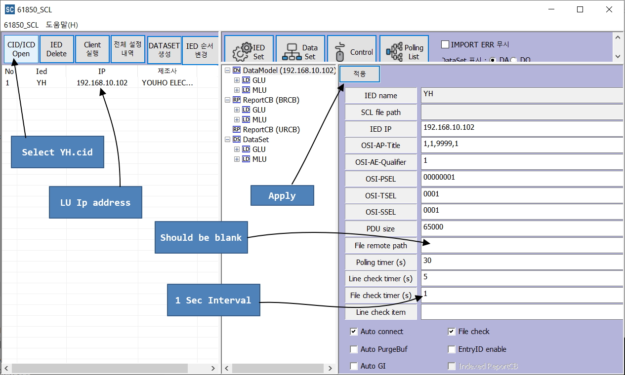
It is required to change settings using SCLManager.exe when required for new setup.
308 parts4

It is required to change settings using SCLManager.exe when required for new setup.
Panel is an open-source printed circuit board by jibonaronno, from the jibonaronno/documentsA repository on GitHub. It is a 2-layer board of 237 × 132.5 mm with 228 parts on 124 nets, routed with 812 tracks and 40 vias.
It is built around the INA219AID, B5PS-VH and MMBT2222A, with the SS14 among its other parts. Its parts include 32 resistors, 28 connectors, 20 diodes, 8 ICs and 4 transistors.


SA_Client.ini has following configs:
LocalIp=192.168.10.105
...
...
PATH=D:/develop/MZAutomation/SAProgram/ClientProc_2017_Dev_NoTimer_Minsu/ClientProc/61850_CFG/CFG/61850/SA_CFG
SAVE_PATH =D:/develop/MZAutomation/SAProgram/ClientProc_2017_Dev_NoTimer_Minsu/ClientProc/61850_CFG/LOG/61850
ENG_PATH =D:/develop/MZAutomation/SAProgram/ClientProc_2017_Dev_NoTimer_Minsu/ClientProc/61850_CFG/DB/ied_info_gw.csv
These configurations should be changed if machine or location is changed.
It is required to change settings using SCLManager.exe when required for new setup.
Confluence Pages From PDA ACQ Operation and calculation / Integration of various current values Copy of 차단기 동작 특성 페이지 https://jlee193.atlassian.net/wiki/spaces/PDA/pages/514129921/Copy+of
Bushing Documentation Page From PDA 부싱 누설 전류 페이지 https://jlee193.atlassian.net/wiki/spaces/PDA/pages/296812597
An Initial Concept of hardware pptx file downloaded in Confluence folder 종합예방진단시스템(20210625)_HW팀.pptx 하드웨어 구성 https://jlee193.atlassian.net/wiki/spaces/PDA/pages/154042616
| Qty | Value | Footprint | References |
|---|---|---|---|
| 124 | NPTH | NPTH | KiKit_MB_10_1, KiKit_MB_10_2, KiKit_MB_10_3, KiKit_MB_10_4, KiKit_MB_11_1, KiKit_MB_11_2, KiKit_MB_11_3, KiKit_MB_11_4, KiKit_MB_12_1, KiKit_MB_12_2, KiKit_MB_12_3, KiKit_MB_12_4, KiKit_MB_13_1, KiKit_MB_13_2, KiKit_MB_13_3, KiKit_MB_13_4 +108 |
| 16 | 470E | Resistor_SMD:R_0603_1608Metric | R3, R3, R3, R3, R4, R4, R4, R4, R5, R5, R5, R5, R6, R6, R6, R6 |
| 16 | LED | LED_THT:LED_D3.0mm | D1, D1, D1, D1, D2, D2, D2, D2, D3, D3, D3, D3, D4, D4, D4, D4 |
| 8 | 4k7 | Resistor_SMD:R_0603_1608Metric | R7, R7, R7, R7, R8, R8, R8, R8 |
| 8 | B5PS-VH | footprints:CONN_B5PS-VH_JST | J2, J2, J2, J2, J3, J3, J3, J3 |
| 8 | Conn_01x07 | Connector_PinSocket_2.54mm:PinSocket_1x07_P2.54mm_Vertical | J4, J4, J4, J4, J5, J5, J5, J5 |
| 8 | Fiducial | Fiducial | KiKit_FID_B_1, KiKit_FID_B_2, KiKit_FID_B_3, KiKit_FID_B_4, KiKit_FID_T_1, KiKit_FID_T_2, KiKit_FID_T_3, KiKit_FID_T_4 |
| 4 | 1K | Resistor_SMD:R_0603_1608Metric | R2, R2, R2, R2 |
| 4 | Conn_01x02 | Connector_PinHeader_2.54mm:PinHeader_1x02_P2.54mm_Vertical | J7, J7, J7, J7 |
| 4 | Conn_01x06 | Connector_PinSocket_2.54mm:PinSocket_1x06_P2.54mm_Vertical | J6, J6, J6, J6 |
| 4 | DCJ200-10-A-XX-K_REVA | DCJ200-10-A-XX-K_REVA:GCT_DCJ200-10-A-XX-K_REVA | J1, J1, J1, J1 |
| 4 | FINDER-36.11 | Relay_THT:Relay_SPDT_Finder_36.11 | K2, K2, K2, K2 |
| 4 | INA219 | INA219:MODULE_INA219 | U2, U2, U2, U2 |
| 4 | MMBT2222A | Package_TO_SOT_SMD:SOT-23 | Q1, Q1, Q1, Q1 |
| 4 | R_Small | Resistor_SMD:R_0603_1608Metric | R1, R1, R1, R1 |
| 4 | SS14 | Diode_SMD:D_SMA | D6, D6, D6, D6 |
| 4 | YAAJ_DCDC_StepDown_LM2596 | KiCad:YAAJ_DCDC_StepDown_LM2596 | U3, U3, U3, U3 |
jibonaronno/documentsA
It is required to change settings using SCLManager.exe when required for new setup.

jibonaronno/documentsA
It is required to change settings using SCLManager.exe when required for new setup.

jibonaronno/documentsA
It is required to change settings using SCLManager.exe when required for new setup.

jibonaronno/documentsA
It is required to change settings using SCLManager.exe when required for new setup.

jibonaronno/documentsA
It is required to change settings using SCLManager.exe when required for new setup.

jibonaronno/documentsA
It is required to change settings using SCLManager.exe when required for new setup.

jibonaronno/documentsA
It is required to change settings using SCLManager.exe when required for new setup.

jibonaronno/documentsA
It is required to change settings using SCLManager.exe when required for new setup.

jibonaronno/documentsA
It is required to change settings using SCLManager.exe when required for new setup.

jibonaronno/documentsA
It is required to change settings using SCLManager.exe when required for new setup.

jibonaronno/documentsA
It is required to change settings using SCLManager.exe when required for new setup.

jibonaronno/documentsA
It is required to change settings using SCLManager.exe when required for new setup.


krishharma/aegis-mtstdp
Integer STDP continual-learning core for FPGA (Python golden model + Verilog). Tiny-net co-sim. IMU/power carrier PCB. Tables are simulator results. Not an ASIC.

JGAguado/Smart_Plant
The Smart Plant is a board that can be plugged directly on the soil, close to the plant, that allows the measurement of the environment (soil moisture, environment temperature & illuminance), and presents the…


ChladpavPy/Aero-Zero
I started this project, because I wanted to build fully autonomous ai drone. When I looked at the flight controllers available on the market, they were full of hardware that I just do not need or just that I could not…

CUSail-Navigation/PCB-FA25-SP26
This is a repository containing the PCBs designed during the FA25-SP26 academic year. Due to high compatibility and relative ease of use, all of these files are made with KiCad.

hari-ghatpande/pcb-cat-toy
PCB designed to drive an MG90S servo using an ESP32, driven off of a LiPo battery.
It measures 237 × 132.5 mm and has 2 copper layers, 1.6 mm thick.
228 parts, built around the INA219AID, B5PS-VH, MMBT2222A and SS14. The full list of its parts is on this page, with links to each part's symbol and footprint where PCBKit's library has them.
From the jibonaronno/documentsA repository on GitHub, at the commit this page was made from: the board is KiCads/Research/meshlite2/Panel/untitled.kicad_pcb. PCBKit opens the board in the browser, with nothing to install.
Its repository states no licence, so its author keeps all rights: ask jibonaronno before reusing the design.