


2 layers66 × 41 mm
Plasma Toroid Generator
PJTodd72/Plasma-Toroid-Driver
Version one of the Ki-Cad schematics and PCB layout of the Plasma Toroid generator driver circuits.
15 parts3

Mazzilli-topology ZVS driver — simulated in LTspice, built on a custom PCB and characterized on the bench
ZVS is an open-source printed circuit board by jenatton-Malik, from the jenatton-Malik/zvs-driver repository on GitHub, published under the MIT licence. It is a 2-layer board of 95 × 138 mm with 19 parts on 7 nets, routed with 65 tracks and 0 vias.
It is built around the IRFP260N and UF4007. Its parts include 4 resistors, 4 diodes, 3 capacitors, 2 transistors and 2 connectors.
A Mazzilli-topology Zero-Voltage-Switching driver — simulated, built and characterized on the bench. Built to understand one of the most elegant self-oscillating circuits in power electronics.
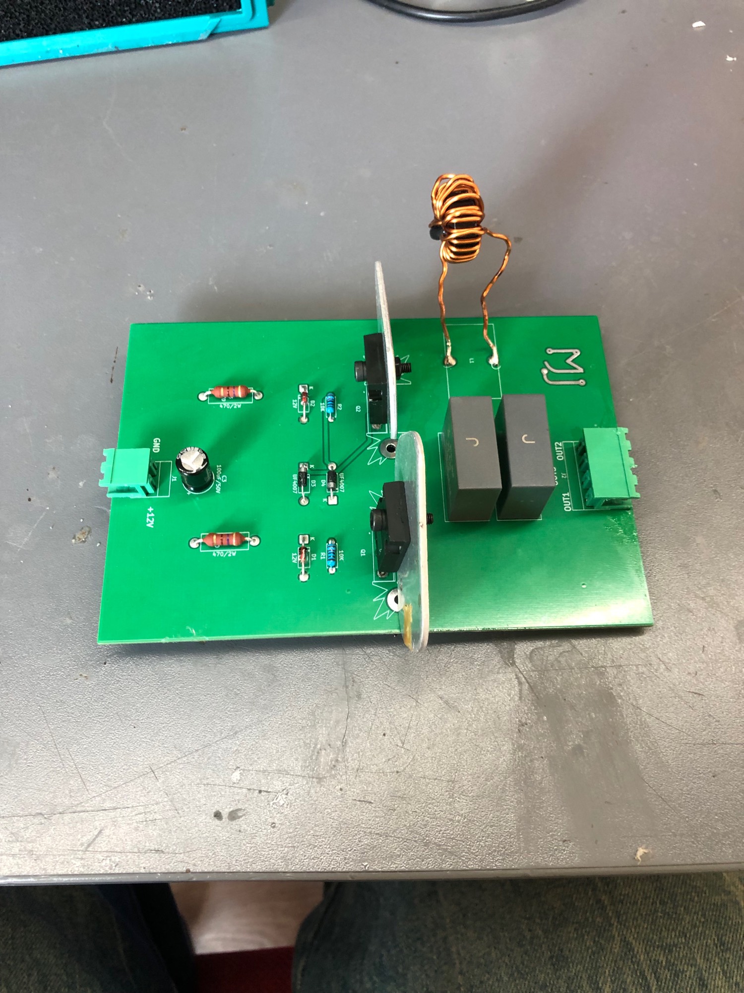
The ZVS looks almost too simple for what it does: two MOSFETs, a handful of passives, no controller, no microcontroller — and it self-oscillates at exactly the right frequency, switching each transistor at the precise moment its drain voltage crosses zero.
I built it to understand why that works. Along the way it also became a working induction heater.
| Topology | Mazzilli ZVS (self-oscillating push-pull) |
| Switching devices | 2 × IRFP260N |
| Rated current | Up to 18 A |
| Tested up to | 8 A |
| Tank capacitors | 2 × 0.33 µF double-metallized film, 9.8 A each |
| Choke | 100 µH |
| Input filtering | 100 µF / 50 V |
| Gate network | 470 Ω / 2 W feed resistors, 10 kΩ pulldowns, 12 V zeners, UF4007 clamp diodes |
On operating frequency: a ZVS has no fixed switching frequency — it's set by the resonant tank, so it depends entirely on the inductance and impedance of whatever work coil is attached. Change the coil, change the frequency. That's the whole point of the topology.
The first step of this project wasn't a soldering iron — it was LTspice. Before touching a single component I simulated the full circuit to understand the oscillation mechanism and verify the passive values.
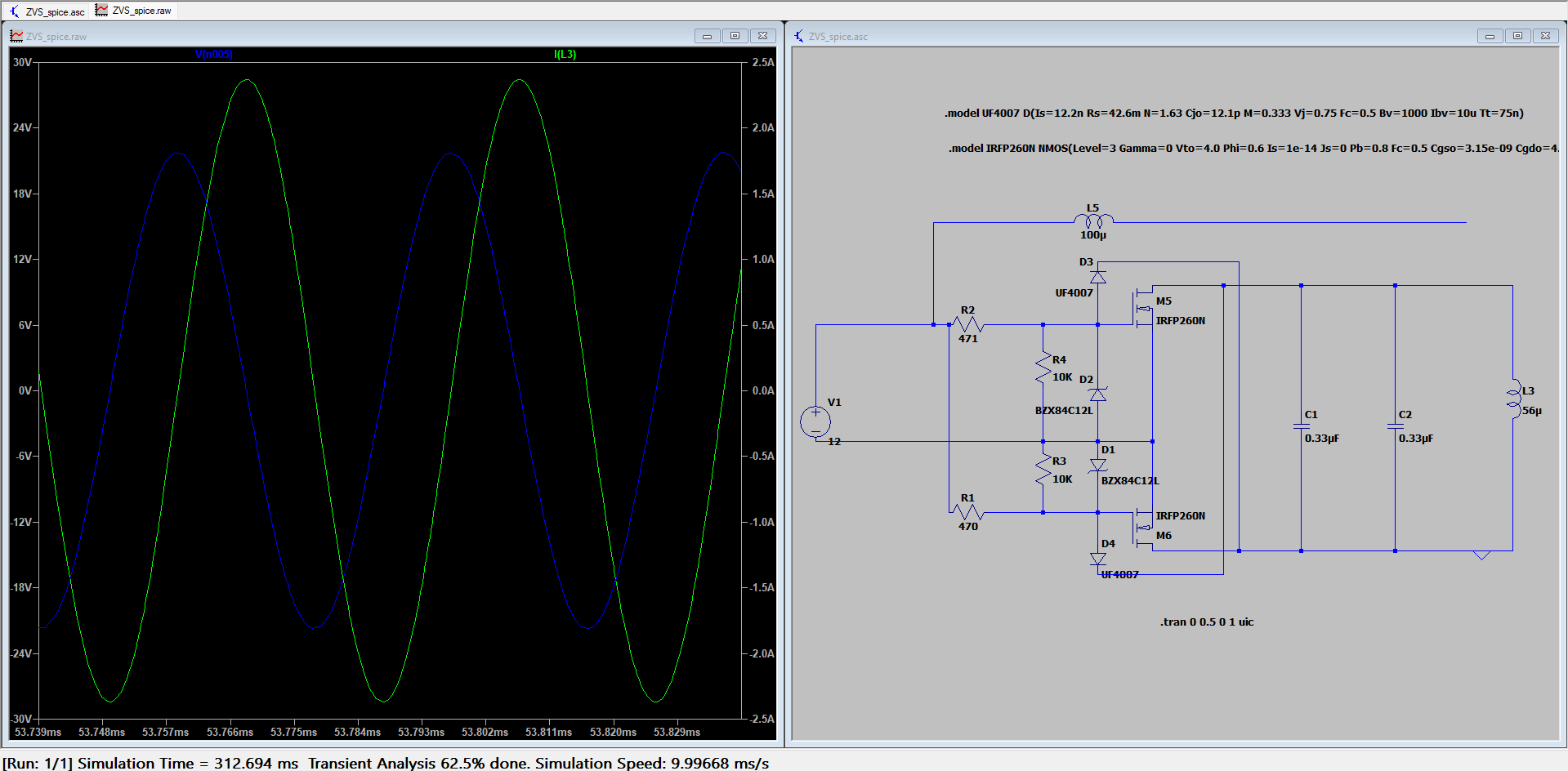
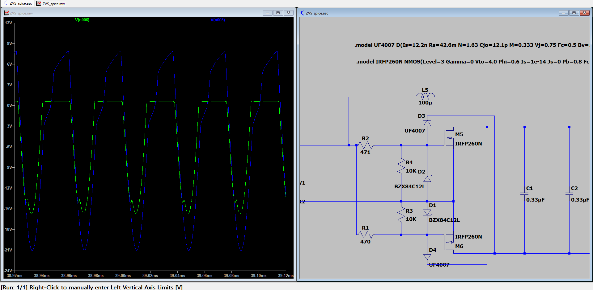
Tank waveform and MOSFET gate drive, simulated in LTspice
The simulation files are in /simulations.
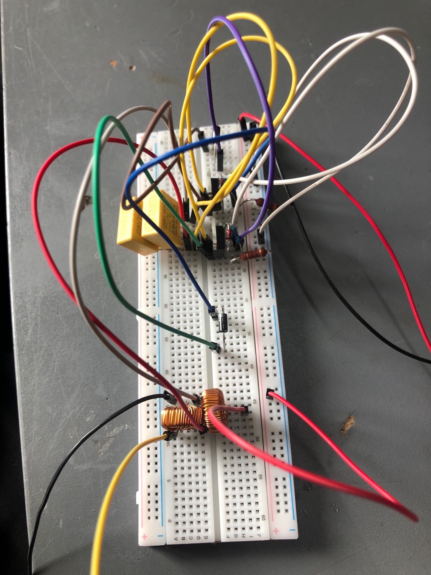
Before committing to a PCB, a smaller version was built on breadboard using IRLZ44N MOSFETs and simple 0.33 µF film capacitors (the mains-filtering type). Lower power, same topology — enough to confirm the circuit oscillates as simulated before spending money on copper.
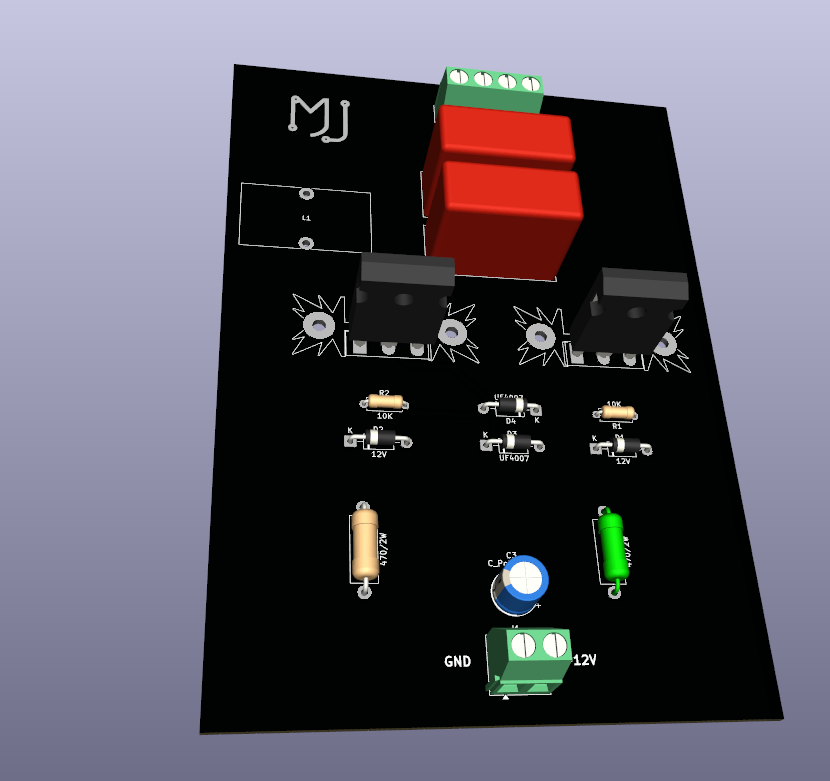
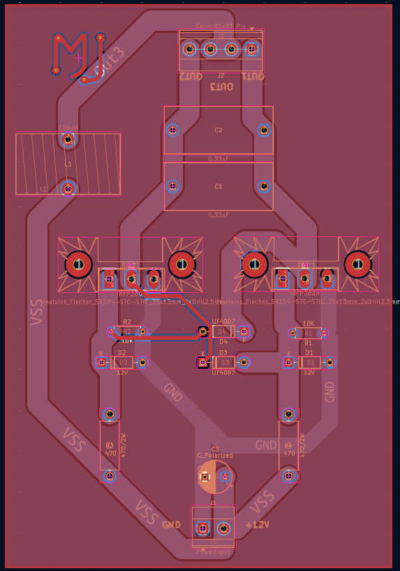
3D render and copper layout — KiCad
Wide, heavy copper pours on the power paths, and generous spacing around the tank — this board carries real current.
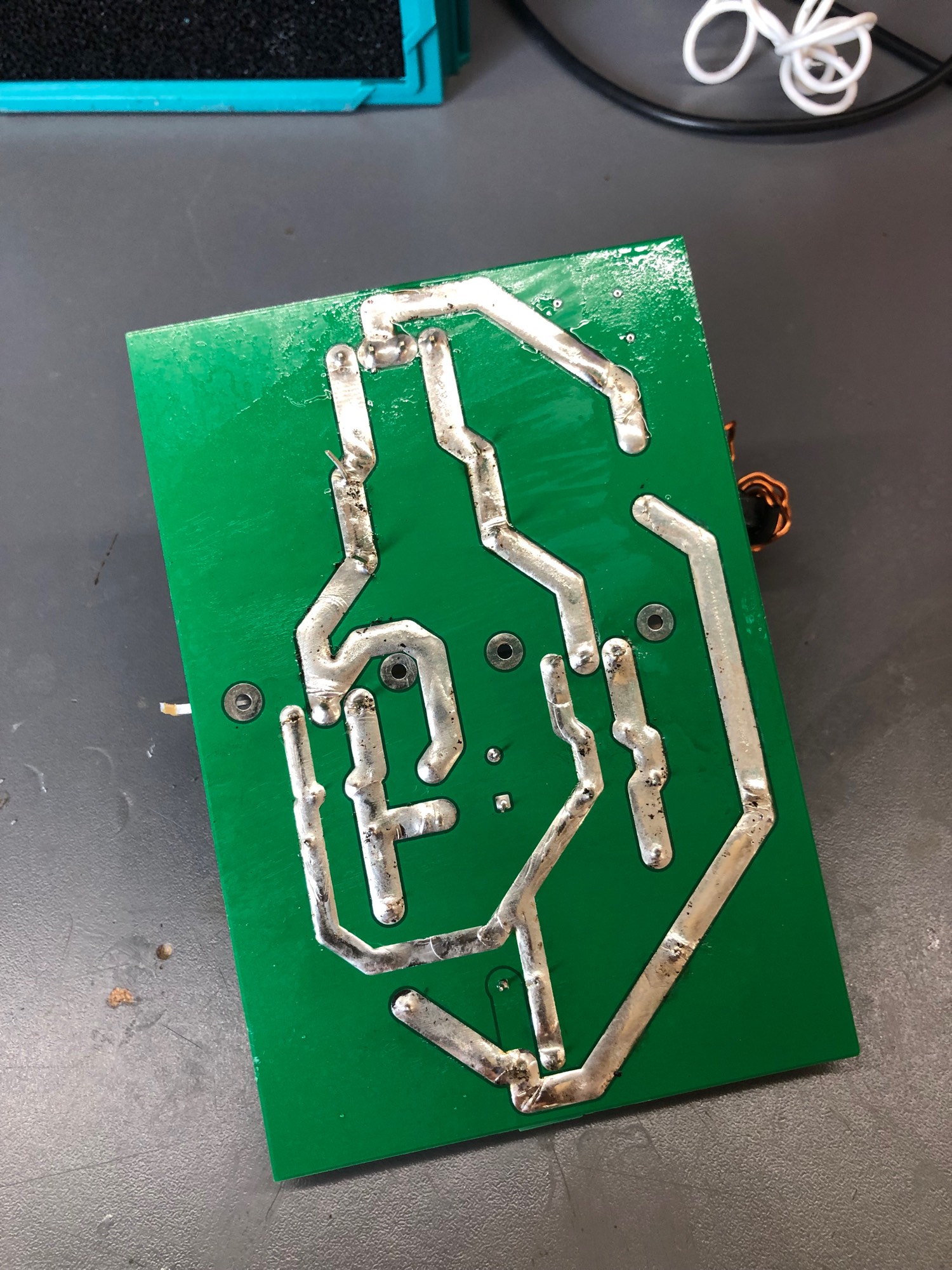
Assembled board, top and bottom
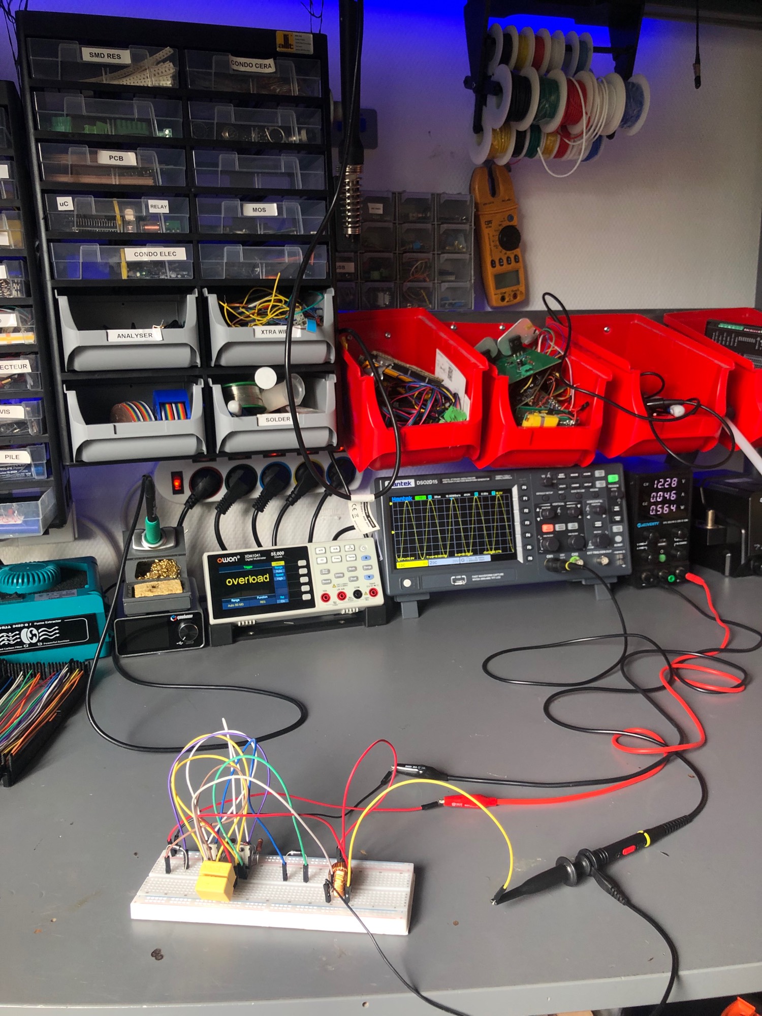
The defining claim of a ZVS is in its name: each MOSFET switches when the voltage across it is at zero, which is why the losses stay so low. So that's what I went looking for on the scope — and confirmed. Switching happens at the zero crossing, exactly as designed.
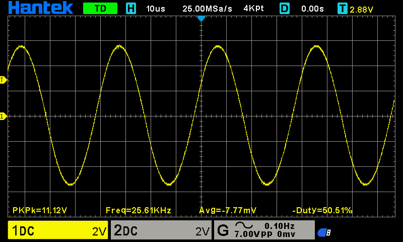
Tank waveform at resonance with a 56 µH work coil
The clean, undistorted sine here is the signature of a tank running properly at resonance — and a direct confirmation of the simulated waveform.
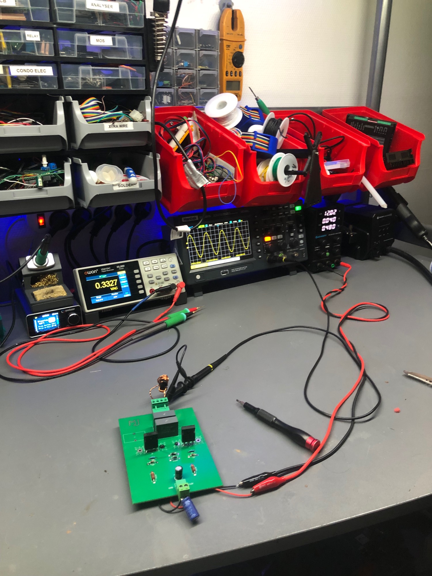
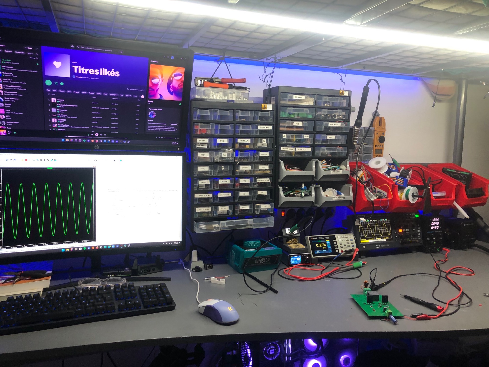
Measuring on the bench — simulation and reality side by side
Thermal behaviour: at just under 10 A, nothing on the board runs hot — not the MOSFETs, not the resistors, not the caps. The components are comfortably sized for the job.
This circuit handles serious power. Even at the currents shown here, the tank voltage across the coil is far higher than the supply voltage, and the components store enough energy to be genuinely dangerous.
I'm interested in eventually driving high-voltage transformers with it — but only with proper equipment and proper supervision. Don't reproduce this unless you know exactly what you're doing.
Built after working through the technical documentation on the topology, along with explainer videos from ElectroBOOM and others in the community who've covered this circuit well.
LTspice · KiCad · Oscilloscope characterization · Power electronics
PCBs manufactured by JLCPCB, as with every board I've designed.
| Qty | Value | Footprint | References |
|---|---|---|---|
| 2 | 0.33uF | Capacitor_THT:C_Rect_L26.5mm_W11.5mm_P22.50mm_MKS4 | C1, C2 |
| 2 | 10K | Resistor_THT:R_Axial_DIN0207_L6.3mm_D2.5mm_P7.62mm_Horizontal | R1, R2 |
| 2 | 12V | Diode_THT:D_DO-41_SOD81_P10.16mm_Horizontal | D1, D2 |
| 2 | 470/2W | Resistor_THT:R_Axial_DIN0414_L11.9mm_D4.5mm_P15.24mm_Horizontal | R3, R4 |
| 2 | IRFP260N | Package_TO_SOT_THT:TO-247-3_Vertical | Q1, Q2 |
| 2 | UF4007 | Diode_THT:D_DO-41_SOD81_P10.16mm_Horizontal | D3, D4 |
| 1 | 100uH | Inductor_THT:L_Toroid_Vertical_L25.4mm_W14.7mm_P12.20mm_Vishay_TJ5_BigPads | L1 |
| 1 | C_Polarized | Capacitor_THT:CP_Radial_D8.0mm_P5.00mm | C3 |
| 1 | Conn_01x03_Pin | TerminalBlock_Phoenix:TerminalBlock_Phoenix_MKDS-1,5-4-5.08_1x04_P5.08mm_Horizontal | J2 |
| 1 | LOGO | Mlabs_F_CU_logo_pcb:logo3 | G*** |
| 1 | PowerInput | TerminalBlock_Phoenix:TerminalBlock_Phoenix_MKDS-1,5-2-5.08_1x02_P5.08mm_Horizontal | J1 |
The 17 most common of 19 parts.
PJTodd72/Plasma-Toroid-Driver
Version one of the Ki-Cad schematics and PCB layout of the Plasma Toroid generator driver circuits.


0hasant/Liion_Cell_Simulator
Single-cell characterization bench for 18650 and 21700 Li-ion cells (DMEGC INR45E, generic 3.5 Ah 18650). Part of the Solaris final-year project.


Firestorm108/Plasma-Speakers-V2
Dual flyback transformers that produce audio through the modulation of high frequency plasma arcs.


Froggy111/RBC-soccer-2025
software and hardware for team BotByWire, Robocup Junior Soccer Lightweight 2025

It measures 95 × 138 mm and has 2 copper layers, 1.6 mm thick.
19 parts, built around the IRFP260N and UF4007. The full list of its parts is on this page, with links to each part's symbol and footprint where PCBKit's library has them.
From the jenatton-Malik/zvs-driver repository on GitHub, at the commit this page was made from: the board is hardware/ZVS.kicad_pcb and its schematic hardware/ZVS.kicad_sch. PCBKit opens the board in the browser, with nothing to install.
Its repository publishes it under the MIT licence: you may reuse it on that licence's terms (keep the author's notice, and for a copyleft licence share your changes alike).