4 layers69 × 74 mm

 imihajlow/ethernet-to-spi69
An Ethernet to SPI converter using 7400-series ICs
Bytesync is an open-source printed circuit board by imihajlow, from the imihajlow/ethernet-to-spi repository on GitHub. It is a 2-layer board of 64 × 28 mm with 17 parts on 17 nets, routed with 117 tracks and 9 vias.
It is built around the 74HC74D and 74HC08D. Its parts include 10 connectors, 3 capacitors and 3 ICs.

The Nucleo64 shield schematic files are located in sch/shield/.
The firmware for stm32f401 is located in stm32eth-f401/.
The idea is to convert the Manchester-encoded 10BASE-T signal to SPI and use an STM32 MCU to parse it.
A 75C1168 chip is used to convert differential signals to 5V logic levels.
Then, edges are detected using a 74HC86 XOR.
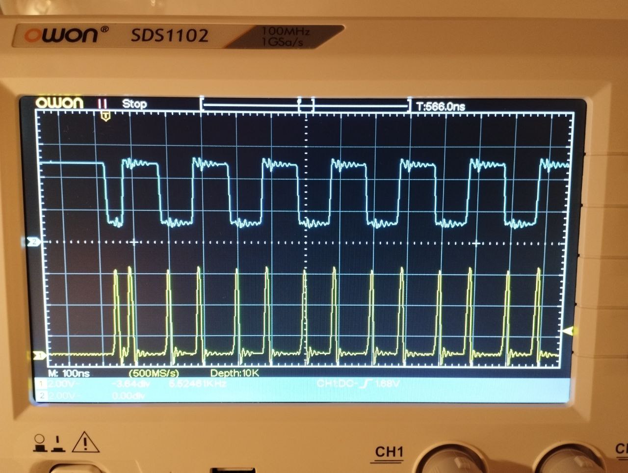
Blue is the input signal, yellow - detected edges.
Then, an ~idle signal is formed using a delay circuit. It goes from 0 to 1 with the first edge and goes back to 0 after approximately 2 µS after the last transition. This signal is used by the MCU to detect the end of an Ethernet frame.
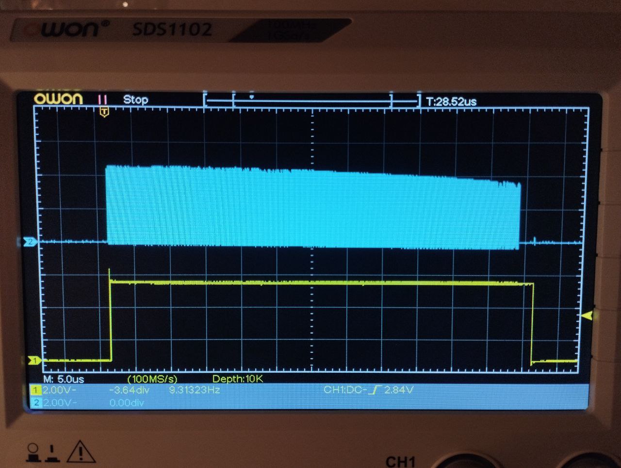
When the line is idle, the output of an 75C1168 is undefined. In my case it was always high. Since the Ethernet frame always starts with a pattern of 101010..., this leads to the first transition always being from 1 to 0, which generates the first edge. This edge must be ignored for SPI clock generation. However, the case with a low idle state needs to be handled as well. In that case the line remains low on the frame begin and the first edge should not be ignored.
The filtering of the first edge is done using the already generated ~idle signal.
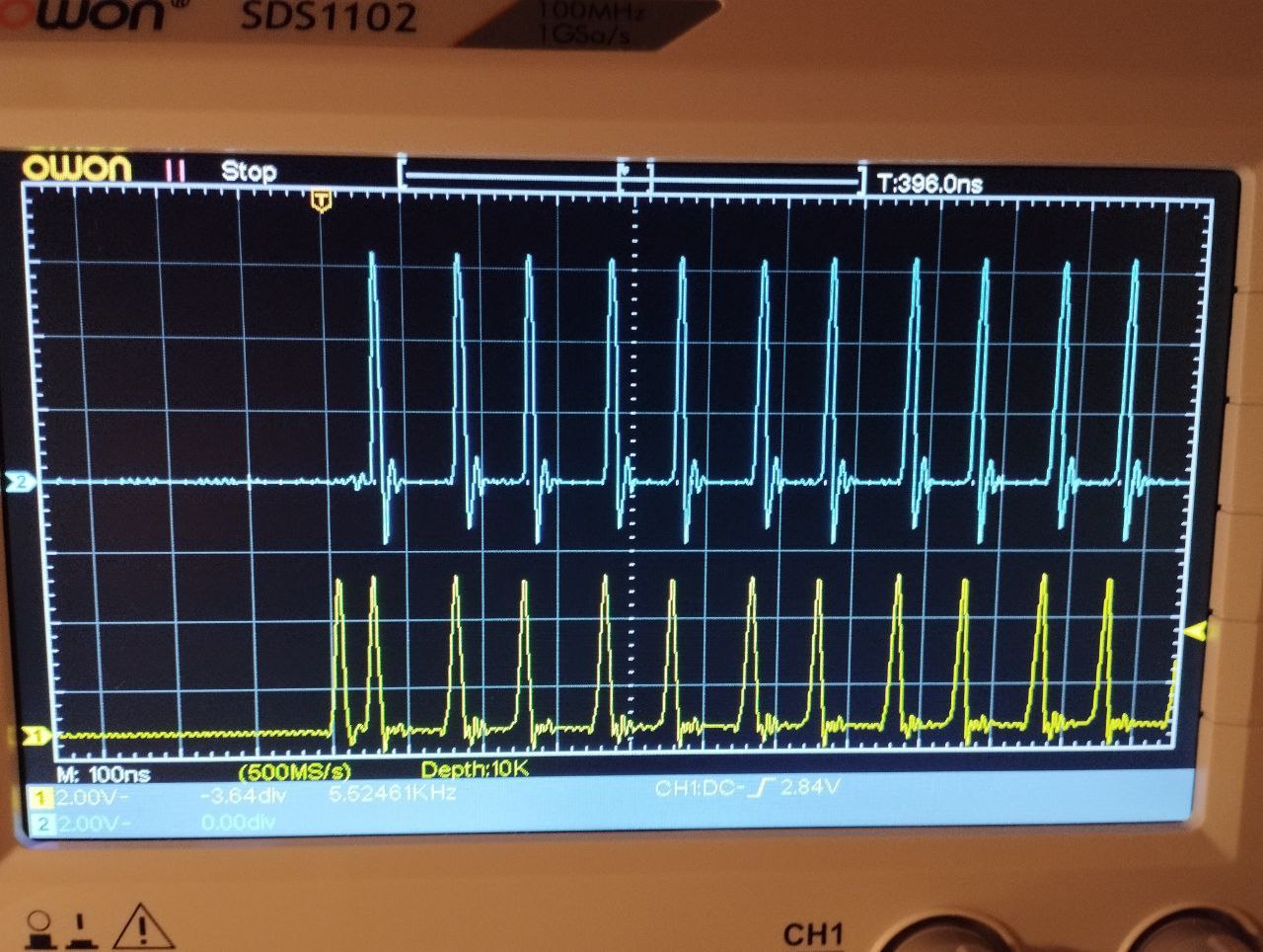
First edge is filtered
The resulting filtered edge signal is fed onto a non-retriggerable monostable circuit which generates a pulse of approximately 75 nS, which is finally used as an SPI clock.
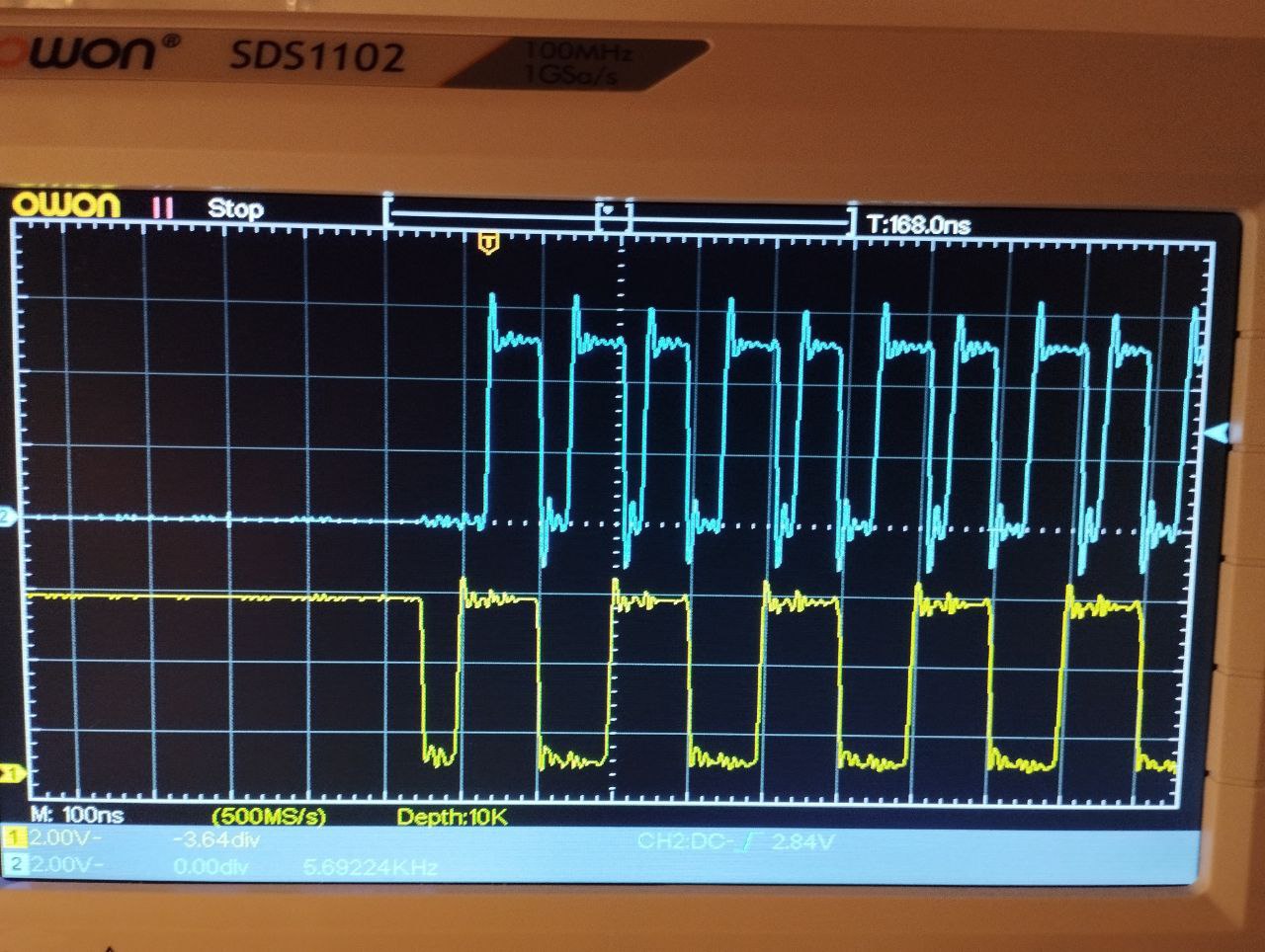
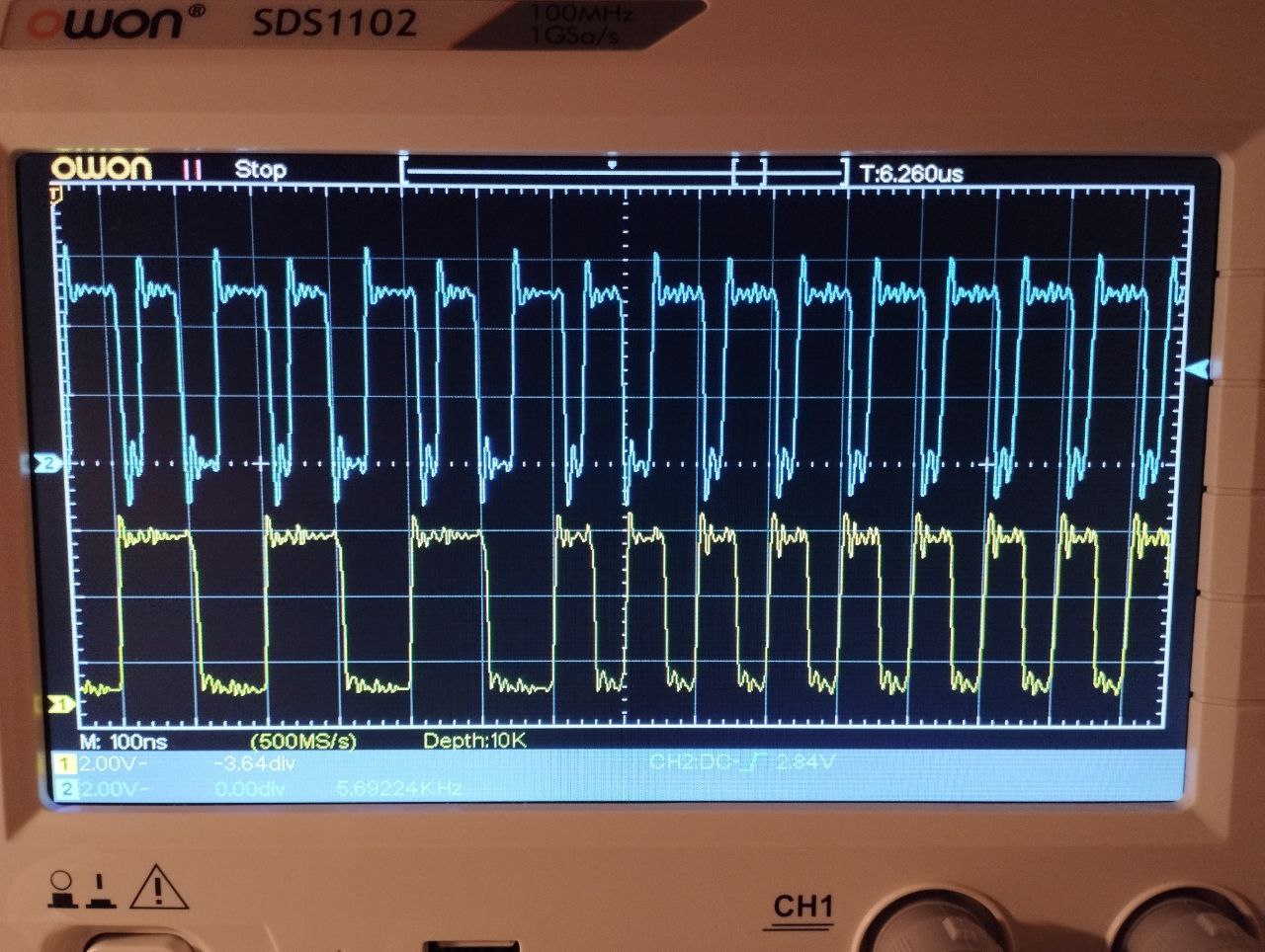
Blue - generated SPI SCK signal, yellow - SPI MOSI which is just the input 10BASE-T signal.
| Qty | Value | Footprint | References |
|---|---|---|---|
| 3 | 0.1 | Capacitor_SMD:C_0805_2012Metric | C1, C2, C3 |
| 2 | 74HC74 | Package_SO:SOIC-14_3.9x8.7mm_P1.27mm | U1, U2 |
| 2 | GND | Connector_Wire:SolderWire-0.75sqmm_1x01_D1.25mm_OD2.3mm_Relief | J6, J7 |
| 2 | VCC | Connector_Wire:SolderWire-0.75sqmm_1x01_D1.25mm_OD2.3mm_Relief | J4, J5 |
| 1 | 74HC08 | Package_SO:SOIC-14_3.9x8.7mm_P1.27mm | U3 |
| 1 | CS_IN | Connector_Wire:SolderWire-0.75sqmm_1x01_D1.25mm_OD2.3mm_Relief | J3 |
| 1 | MOSI_IN | Connector_Wire:SolderWire-0.75sqmm_1x01_D1.25mm_OD2.3mm_Relief | J1 |
| 1 | MOSI_OUT | Connector_Wire:SolderWire-0.75sqmm_1x01_D1.25mm_OD2.3mm_Relief | J8 |
| 1 | SCK_IN | Connector_Wire:SolderWire-0.75sqmm_1x01_D1.25mm_OD2.3mm_Relief | J2 |
| 1 | SCK_OUT | Connector_Wire:SolderWire-0.75sqmm_1x01_D1.25mm_OD2.3mm_Relief | J10 |
| 1 | SYNC | TestPoint:TestPoint_Pad_D2.0mm | TP1 |
| 1 | ~{CS_OUT} | Connector_Wire:SolderWire-0.75sqmm_1x01_D1.25mm_OD2.3mm_Relief | J9 |

imihajlow/ethernet-to-spi
An Ethernet to SPI converter using 7400-series ICs


artemisamsx/artemisa
Schematics, PCB designs and HDL simulations to build a 8-bits MSX computer


46nori/Z80Atmega128
Real Z80A system with I/O emulated by AVR(ATmega128)

EwoudVV/arpeggiator
12-note analog arpeggiator with a 1/2/3 octave range, custom pcb and printed case

It measures 64 × 28 mm and has 2 copper layers, 1.6 mm thick.
17 parts, built around the 74HC74D and 74HC08D. The full list of its parts is on this page, with links to each part's symbol and footprint where PCBKit's library has them.
From the imihajlow/ethernet-to-spi repository on GitHub, at the commit this page was made from: the board is sch/bytesync/bytesync.kicad_pcb and its schematic sch/bytesync/bytesync.kicad_sch. PCBKit opens the board in the browser, with nothing to install.
Its repository states no licence, so its author keeps all rights: ask imihajlow before reusing the design.