


2 layers54 × 85.6 mm
Board43
smartbank-inc/Board43
Board43 is an RP2350A-based microcontroller development board. Flash PicoRuby or your favorite firmware and start hacking.
583 parts30
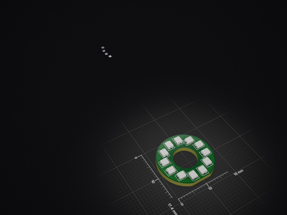
 HeyPCB/iris-ring
Iris Ring: the 18 mm annular LED board behind each iris of the Iris robot head. 12 WS2812-2020 pixels around the camera lens. 2-layer, 0.8 mm KiCad 10 board, DRC-clean, with gerbers, BOM, CPL, STEP and renders.
Iris ring is an open-source printed circuit board by HeyPCB, from the HeyPCB/iris-ring repository on GitHub, published under the CERN-OHL-S-2.0 licence. It is a 2-layer board of 18 × 17.4 mm with 30 parts on 16 nets, routed with 225 tracks and 10 vias.
It is built around the WS2812C-2020-V1. Its parts include 13 capacitors, 12 diodes, 4 connectors and 1 resistor. It belongs with the robots and motor control and lEDs and displays boards of this library.
The annular LED board behind each iris of Iris: 12 WS2812-2020 pixels on an 18 mm ring around the camera lens, two per head.
Part of Iris, the human-eyed robot head, HeyPCB's open robot boards. Designed end to end with the HeyPCB method on
KiCad 10 (headless pipeline, Freerouting 2.4.1); every number below is measured on the files in this repository.
Mentions of ./run.sh, docs/rules/, blocks/ or parts/ refer to the heypcb-kicad SDK that produced them.
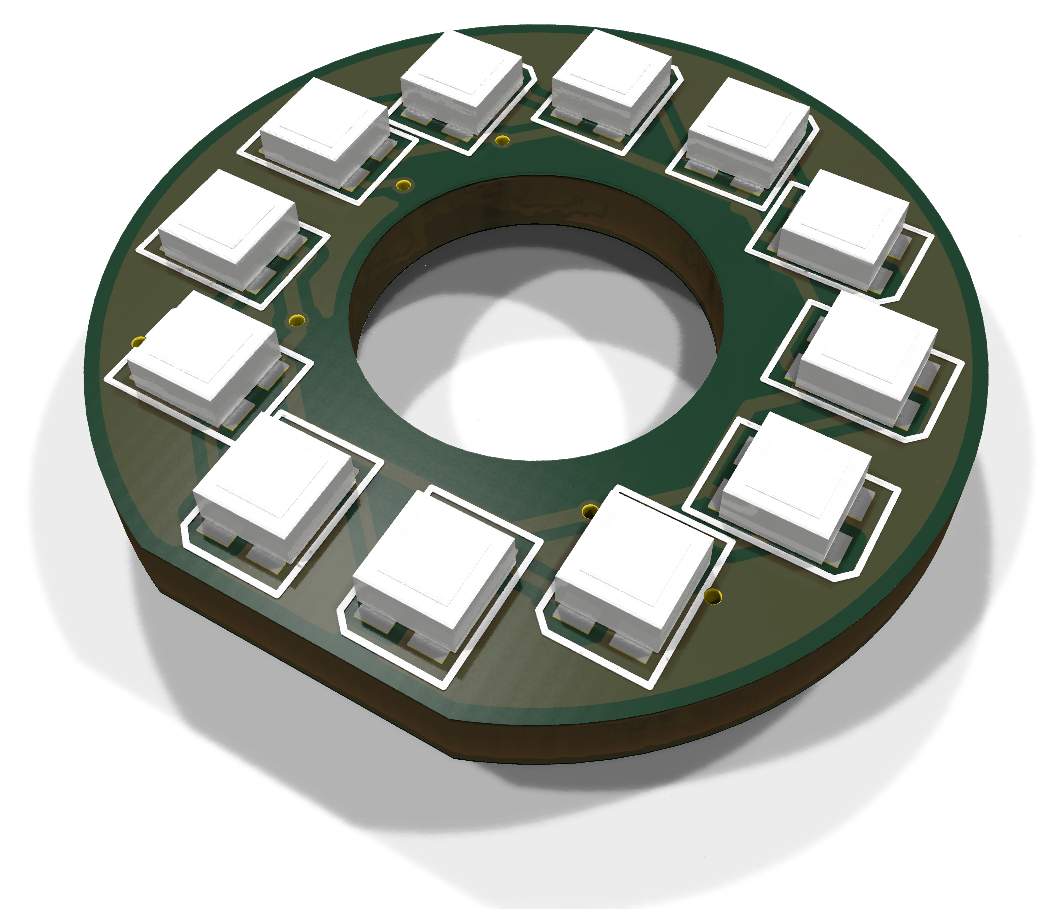
| Layers | Outline | Parts | Nets | Connections routed | Vias | ERC errors | DRC errors / unconnected / parity |
|---|---|---|---|---|---|---|---|
| 2 | 18 x 18 mm, shaped with 1 cutout | 30 | 15 | 64 -> 0 open | 10 | 0 | 0 / 0 / 0 |
Not fabricated, assembled or powered.
| KiCad project | kicad/ |
| Gerbers (unzipped and zipped), BOM, CPL, STEP, schematic PDF | fab/ |
| Mechanism CAD, fit check and system docs | Iris, the human-eyed robot head |
| Renders | top, bottom |
| Design process, every step as KiCad rendered it | media/design-process.mp4 |
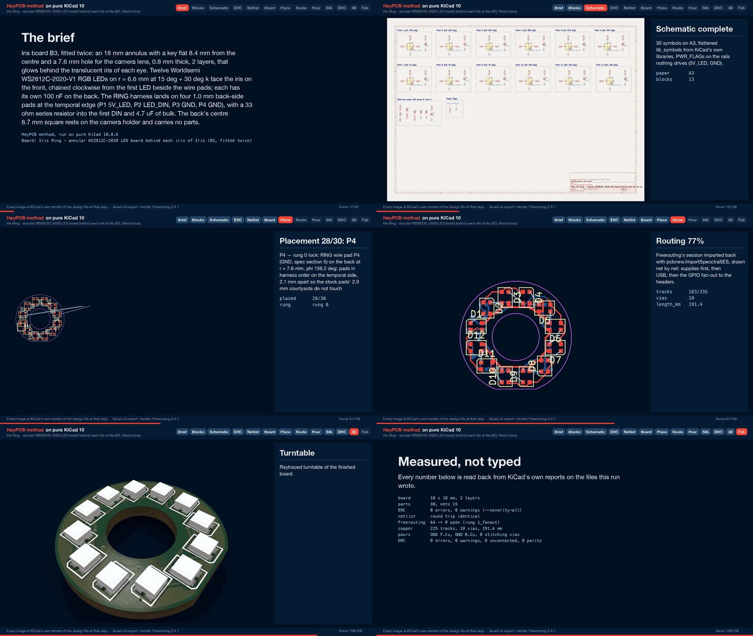
Iris Ring is the annular LED board that glows behind each iris of Iris, an open-hardware robot
head with human eyes. Each head carries two identical boards, one per eye. Each is an 18 mm disc with
a key flat and a 7.6 mm hole for the camera lens, and it carries twelve WS2812C-2020 RGB LEDs. It was
designed with the HeyPCB method on KiCad 10 (the headless heypcb-kicad pipeline, KiCad 10.0.6,
routed by Freerouting 2.4.1). The brief, board.json, is written by make_brief.py and follows
section 4.4 (B3) and section 5 (interconnect contracts) of the Iris system spec v0.1 (not
published; the contracts are in the Iris system docs).
It has not been fabricated, assembled or powered. Every gate number below comes from the final
run's report.json (2026-10-03, ./run.sh --board boards/iris_ring with media,
from an empty build directory). Copper, pad and position numbers were read from
kicad/iris_ring.kicad_pcb with KiCad 10.0.6's pcbnew. Thickness and heights were read
from the solids of fab/iris_ring.step. Datasheet facts are cited by page under
Licence and sources.
| Front (LED face) | Back (camera side) |
|---|---|
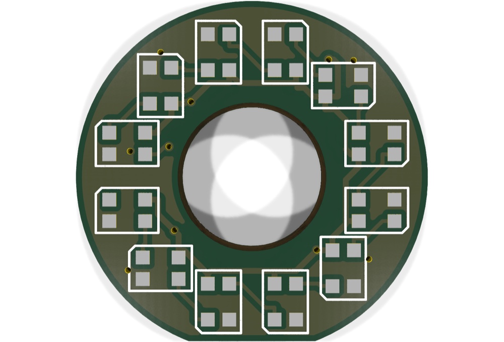 | 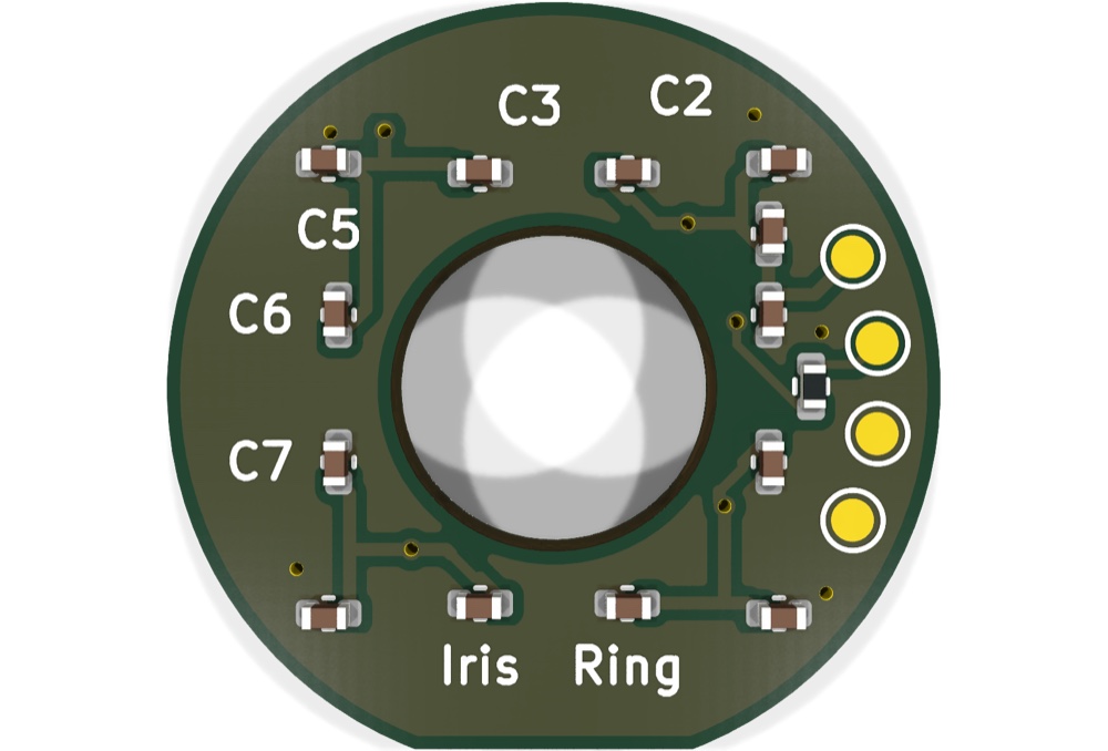 |
The renders show the LED lands without LED bodies, because KiCad 10.0.6 ships no 3D model for
LED_WS2812B-2020_PLCC4_2.0x2.0mm. They also show a 1.6 mm board, not 0.8 mm (see Check before
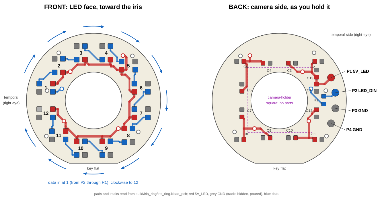
ordering). draw_map.py draws the map from the routed board.
The ring sits inside each 30 mm eyeball, between the camera and the translucent iris disc. It lights the iris from behind for gaze and mood cues. B1 Cortex drives it from its RMT peripheral (GPIO47 and GPIO48, 800 kHz, spec section 8) through a 74AHCT1G125 at 5 V.
Eye stack-up along the optical axis, x from the eye centre (spec section 2.2; design values, not measured on hardware):
| x (mm) | Part |
|---|---|
| 4.36 to 7.01 | OV2640 camera module (right eye) or dummy carrier (left eye); the ring's back rests on the holder top |
| 7.0 to 7.8 | Iris Ring: back face 7.0, front face 7.8 (0.8 mm board) |
| 7.8 to 8.64 | WS2812C-2020 bodies, 0.84 mm (catalogue row) |
| 7.01 to 9.01 | camera lens barrel, Ø7.2, through the ring's Ø7.6 hole |
| 9.01 to 9.90 | lens front step, Ø5.4, inside the black pupil sleeve (ID 5.6) |
| 8.65 to 11.1 | light-mixing cavity, painted white inside |
| 11.1 to 11.9 | translucent iris disc, Ø14.6, pupil hole Ø5.6 |
| up to 16.40 | clear cornea dome (apex) |
Orientation in the head. The board frame used below has its origin at the ring centre, +x away from the wire pads and +y toward the key flat, seen from the front.
Outline as built (read from Edge.Cuts):
The polygon's corners are where tangents of the circle meet, so their 9 mm fillets are exact arcs and nothing is faceted.
2 layers, 0.8 mm (an order option; see Check before ordering). GND is poured on both faces after routing measured 0 open.
12 x Worldsemi WS2812C-2020-V1 (C2976072) on the front on r = 6.600 mm, every 30° from 15°, data chained clockwise.
One 100 nF per LED (12 x 0402, C1525) on the back, plus 4.7 uF bulk (0402, C23733) and a 33 ohm DIN series resistor (0402, C25105).
Four 1.0 mm wire pads on the back, at the temporal edge, for the RING harness (P1 5V_LED, P2 LED_DIN, P3 GND, P4 GND).
No parts in the back's centre 8.7 x 8.7 mm square, where the board rests on the camera holder (a footprint keepout on B.Cu, spec 4.4). Tracks and vias may pass under it.
Heights.
No holes. The carrier's seat and the iris disc's rim clamp the board, and the flat keys its rotation.
P2 LED_DIN -> R1 33 ohm -> D1 -> D2 -> D3 -> ... -> D11 -> D12 (D12 DOUT is not connected)| LED | Angle | Centre (x, y) mm | LED | Angle | Centre (x, y) mm |
|---|---|---|---|---|---|
| D1 | 195° | (-6.375, -1.708) | D7 | 15° | (6.375, 1.708) |
| D2 | 225° | (-4.667, -4.667) | D8 | 45° | (4.667, 4.667) |
| D3 | 255° | (-1.708, -6.375) | D9 | 75° | (1.708, 6.375) |
| D4 | 285° | (1.708, -6.375) | D10 | 105° | (-1.708, 6.375) |
| D5 | 315° | (4.667, -4.667) | D11 | 135° | (-4.667, 4.667) |
| D6 | 345° | (6.375, -1.708) | D12 | 165° | (-6.375, 1.708) |
Angles are measured from +x toward +y, which is clockwise seen from the front. Every centre is at r = 6.600 mm.
LED orientation. Each LED is turned so that DOUT and GND face the rim and DIN and VDD face the hole, with DOUT on the clockwise side. Data then hops from one LED's outer DOUT to the next LED's inner DIN, and no hop crosses a supply connection. The SDK places parts in quarter turns only, so each LED faces the axis nearest its radius. The four diagonal LEDs (D2, D5, D8, D11) take their clockwise neighbour's turn. That gives 2.56 and 1.86 mm from DOUT pad centre to DIN pad centre; the other choice gives 4.00 and 3.33 mm.
RING_R runs from B1 J2 to the right eye's ring, and RING_L from B1 J3 to the left eye's ring. Each is a JST SH-4 (SM04B-SRSS-TB) at B1, then four 32 AWG silicone wires, 100 mm, soldered to the pads below.
| B1 pin | B3 pad | Net | Direction | Level |
|---|---|---|---|---|
| 1 | P1 | 5V_LED | B1 -> B3 | 5V_SYS through a 0.5 A PTC or ferrite on B1 (4.85 V nominal at B1's input); the source is B2, via B1 |
| 2 | P2 | LED_DIN | B1 -> B3 | 5 V CMOS from 74AHCT1G125, WS2812 protocol at 800 kHz |
| 3 | P3 | GND | — | |
| 4 | P4 | GND | — |
Pad centres on the back, measured, in mm from the ring centre (board frame, as seen from the front):
| Pad | Board (x, y) | Right eye (Y, Z) | Left eye (Y, Z) |
|---|---|---|---|
| P1 5V_LED | (-6.952, -3.070) | (-6.952, +3.070) | (+6.952, -3.070) |
| P2 LED_DIN | (-7.527, -1.050) | (-7.527, +1.050) | (+7.527, -1.050) |
| P3 GND | (-7.527, +1.050) | (-7.527, -1.050) | (+7.527, +1.050) |
| P4 GND | (-6.952, +3.070) | (-6.952, -3.070) | (+6.952, +3.070) |
From the WS2812C-2020-V1 datasheet: 5 mA per colour channel (p.1, and the LED test condition on p.3), and 0.5 mA quiescent per LED (p.3). Power is at 4.85 V, H1's nominal 5V_SYS (spec section 5); the drop in B1's PTC or ferrite and in the harness is not counted.
| State | Current | Power |
|---|---|---|
| Full white: 12 x (3 x 5 mA + 0.5 mA) | 186 mA | 0.90 W |
| Firmware cap, 30 % brightness (spec section 8): 0.3 x 180 mA + 6 mA | 60 mA | 0.29 W |
| All dark: 12 x 0.5 mA | 6 mA | 29 mW |
| One LED at full white | 15.5 mA | 75 mW |
route.ipc2221_amps), 0.225 mm carries 0.81 A and 0.3 mm carries 1.00 A: four times the full-white current or more.| Gate | Result |
|---|---|
| Composition | 13 block instances (12 irisring_pixel, 1 irisring_wire_in) -> 30 parts, 15 nets, 1 no-connect (D12 DOUT) |
Part binding (parts/lcsc_pinned.json) | 26 of 26 BOM parts bound, 0 unsourced, 0 identity conflicts; the four wire pads are do-not-populate (nothing to buy). 1 distinct Extended part (the LED), about $3 in JLC loading fees |
ERC (kicad-cli sch erc --severity-all) | 0 errors, 0 warnings |
| Netlist round trip | identical, 15 nets |
| Freerouting, rung 1, fanout on (kept) | 64 -> 1 open; the last mile closed it (GND, D10.2 to C1.2, 3.16 mm, no via; kept by DRC): 0 open, DRC score 0 |
| Freerouting, rung 1, fanout off (measured for comparison) | 64 -> 1 open (DIN11, D10.1 to D11.3); the last mile found no path. DRC score 1 |
| Copper | 225 tracks, 10 vias (5 GND, 4 5V_LED, 1 DIN1), 191.4 mm of track (F.Cu 105.4, B.Cu 86.0). No class was narrowed |
| Pours (only after a measured 0 open) | GND on F.Cu and B.Cu; 0 stitching vias (no point of the 3 mm lattice fitted); 0 open after the pour and at the end; no island-repair vias |
| Silkscreen | the name, "Iris" and "Ring", placed as 2 words on the back; 5 back designators seated (C2, C3, C5, C6, C7), 23 hidden where nothing fit; nothing clipped |
DRC (--severity-all --schematic-parity, KiCad 10.0.6) | fresh, 0 errors, 0 warnings, 0 unconnected, 0 parity |
DFM (jlcpcb_2layer) | 0 errors, 1 warning (92 stock-footprint silk strokes at 0.12 mm; the fab prints them at its 0.15 mm minimum) |
| Fab gate | ready, no blockers; gerbers for 2 copper layers, drill, BOM, JLC CPL (8 rotations corrected), schematic PDF, STEP |
| Media | renders and the design-process video (108.5 s, 158 frames), in build/iris_ring/ (not committed) |
| The spec says | On the board | Why |
|---|---|---|
| LEDs on r = 6.6 at 15° + 30°·k | Exactly that, every lock computed from its angle (make_brief.py) | Each centre is at r = 6.600 mm (measured) |
| (implied) LEDs turned radially | Quarter turns: each LED faces the axis nearest its radius | The SDK places parts at 0, 90, 180 or 270° only. A lock at 225° stops the place stage with an unnamed ValueError: 225 from place._rot_pt. The positions keep 4-fold symmetry, and so do the data hops |
P1-P4: Connector_Generic:Conn_01x04 on 4 x TestPoint_Pad_D1.0mm, r = 7.35, 1.27 mm pitch | 4 x Connector:TestPoint on TestPoint_Pad_D1.0mm, on r = 7.6, 2.1 mm apart | A 4-pin symbol cannot sit on four 1-pad footprints. The stock footprint's courtyard is a Ø2.0 mm circle, so 1.27 mm pitch is a courtyards_overlap DRC error. The pads keep their Ø1.0 mm and the §5 order |
| C1-C12 on the back at r ≥ 6.3 | 8 at r = 5.28 (C1, C3, C4, C6, C7, C9, C10, C12), lying along the ring under their LED's inner pads; 4 at r = 7.40 on the diagonals (C2, C5, C8, C11) | The inner positions leave the back's band above the key flat free for the board's name, and put each capacitor's 5V_LED pad beside its LED's VDD pad. Every part clears the camera-holder square: make_brief.py checks it, and the keepout's DRC confirms it. On the diagonals the square's corner reaches r = 6.15, so those four stay outside it |
| Copper to edge: not in the spec (the other boards here use 0.5 mm) | 0.3 mm | D9 and D10 come to 0.76 mm from the key flat. At 0.5 mm no ground track fitted below them, the router ran GND between the LEDs, and DIN11 stayed open (measured on this brief). At 0.3 mm it routes to 0 open |
| Board name on the back "if it fits" | "Iris Ring" as two silk words below C9 and C10, in a via-free window | As a title line it found no room: the silk stage seats designators first, and they took the only free band. Words are placed before designators |
BoardThickness 1.6 mm (KiCad's default 2-layer stackup: 0.035 mm copper, 1.51 mm FR4).cad/out/fit.json, board B3): at 0.8 mm the ring seats in the eye carrier under the iris clamp ring with no collision; at the exported 1.51 mm the board overlaps the clamp ring by 21.3 mm³, so the clamp would sit 0.71 mm high.board.json: the brief, written by make_brief.py. Edit the script, not the JSON. The script places every part by formula and checks courtyards, the camera-holder square and the edge clearances before the pipeline runs.make_brief.py: the outline, every lock and the brief (Python 3.9+, standard library only).draw_map.py: the assembly map, img/iris_ring_map.svg, drawn from the routed board (run it under KiCad's Python).img/: KiCad's raytraced renders of both faces and an angled view (iris_ring_3d.jpg), and the map.blocks/irisring_pixel.json (one LED and its 100 nF) and blocks/irisring_wire_in.json (wire pads, 33 ohm, 4.7 uF).parts/lcsc_pinned.json, from live lookups of 2026-10-03.python3 boards/iris_ring/make_brief.py, then ./run.sh --board boards/iris_ring. The outputs land in build/iris_ring/, which is not committed: gerbers, drill, BOM, CPL, schematic PDF and STEP in fab/, and the renders and video.The Iris Ring design files are licensed under the CERN Open Hardware Licence Version 2 -
Strongly Reciprocal (CERN-OHL-S-2.0), https://ohwr.org/cern_ohl_s_v2.txt. They are this
directory, blocks/irisring_pixel.json and blocks/irisring_wire_in.json. KiCad's symbols,
footprints and 3D models are CC-BY-SA-4.0 with the KiCad library exception. No datasheet is copied
into this repository.
LED:WS2812B-2020 symbol (1 DOUT, 2 VSS, 3 DIN, 4 VDD);| Qty | Value | Footprint | References |
|---|---|---|---|
| 12 | 100nF | Capacitor_SMD:C_0402_1005Metric | C1, C2, C3, C4, C5, C6, C7, C8, C9, C10, C11, C12 |
| 12 | WS2812C-2020-V1 | LED_SMD:LED_WS2812B-2020_PLCC4_2.0x2.0mm | D1, D2, D3, D4, D5, D6, D7, D8, D9, D10, D11, D12 |
| 2 | GND | TestPoint:TestPoint_Pad_D1.0mm | P3, P4 |
| 1 | 33 | Resistor_SMD:R_0402_1005Metric | R1 |
| 1 | 4.7uF | Capacitor_SMD:C_0402_1005Metric | C13 |
| 1 | 5V_LED | TestPoint:TestPoint_Pad_D1.0mm | P1 |
| 1 | LED_DIN | TestPoint:TestPoint_Pad_D1.0mm | P2 |
It measures 18 × 17.4 mm and has 2 copper layers, 1.6 mm thick.
30 parts, built around the WS2812C-2020-V1. The full list of its parts is on this page, with links to each part's symbol and footprint where PCBKit's library has them.
From the HeyPCB/iris-ring repository on GitHub, at the commit this page was made from: the board is kicad/iris_ring.kicad_pcb and its schematic kicad/iris_ring.kicad_sch. PCBKit opens the board in the browser, with nothing to install.
Its repository publishes it under the CERN-OHL-S-2.0 licence: you may reuse it on that licence's terms (keep the author's notice, and for a copyleft licence share your changes alike).
smartbank-inc/Board43
Board43 is an RP2350A-based microcontroller development board. Flash PicoRuby or your favorite firmware and start hacking.


ItsNotDaan/LiberBoard
LiberBoard: An open-source, modular platform for learning electronics. Offers LiBo ARM-based PCBs and add-on boards with practical exercises and code snippets. Designed for easy learning and project creation.

cepetr/blue2joy
Bluetooth HID adapter for Atari 8-bit computers: use modern BLE gamepads or mice to emulate the Atari joystick and paddles.

botanicfields/PCB-RGB-LED-276-M5Atom
Circle clock using 276pcs of WS2812C-2020 and an M5Atom