
2 layers79 × 83 mm

 Guiimartinho/open-power-profiler
Open-source PPK2-class power profiler built on the Raspberry Pi Pico 2: 100 kSPS, 100 nA to 1 A auto-ranging, source meter and ampere meter modes, USB stream.
Power profiler carrier is an open-source printed circuit board by Guiimartinho, from the Guiimartinho/open-power-profiler repository on GitHub, published under the MIT licence. It is a 4-layer board of 150 × 100 mm with 425 parts on 258 nets, routed with 3,743 tracks and 694 vias.
It is built around the OPA197IDBV, OPA365AIDBV and TC4427EOA713, with the TPD4E1U06DBVR, LP5907MFX-3.3/NOPB(MS) and SN74LV165ADRE4 among its other parts. Its parts include 114 resistors, 108 capacitors, 21 ICs, 19 diodes and 16 transistors. It belongs with the sensors and measurement boards and the RP2040 and RP2350 boards of this library.





Open-source power profiler in the class of the Nordic PPK2, built around the Raspberry Pi Pico 2. It is designed to sample current at 100 kSPS from 100 nA to 1 A with automatic range switching, to work either as a source meter that powers the device under test or as an ampere meter in series with an external supply, and to stream the samples to a PC over USB.
The instrument is two boards: a Raspberry Pi Pico 2, bought ready-made, plugged into a carrier board designed in this project that holds the measurement electronics.
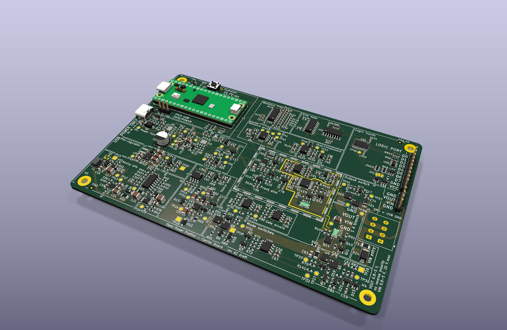
The picture is a rendering from the KiCad files of draft A2, with the Pico 2 on its sockets. It is not a photograph: no board has been built.
[!NOTE] The project is in early development. No hardware has been built and nothing has been measured. The performance figures in this repository are design targets, the circuits of the board are simulated from its netlist, and the figures of the board are calculated from the drawn copper. Project Status says what exists, what it rests on and what comes next.
As of 2026-10-13. Draft A2 of the carrier board is the present state of the hardware: the whole schematic, a specification written for it, and a board with every part placed and every one of its 984 connections drawn. The board was first routed by an autorouter, which left 28 connections open. Its layout has since been reviewed: the open connections are closed and the copper that an autorouter does not draw is drawn, the pours of the 1 A path, the guard, the sense pairs and the copper of the converters. The review was done with scripts and checked by independent calculation. The seven points where the reviewed board departs from the first wording of section 10 of the specification are recorded decisions, D-87 to D-93, and the specification follows them.
On 2026-10-13 a person looked at the drawings for the first time: the
project owner opened the schematic and the board in the KiCad editor and
found both coherent. It was a look, not a review item by item, and no
edit was saved. The same day the footprints and the placement were
reviewed on a copy of the project, with scripts on the board file, 3D
renderings of every region of the board and the datasheets. Five findings
of that review were worked into the board at single points, with no new
routing, and the silkscreen got the frames and names of the functional
blocks
(Review of Footprints and Placement).
What is open is the review of the board item by item in the KiCad
editor, a list of items that need parts moved, what the silkscreen and
the test points still lack, and the thermal check of D-93.
Every figure of the board is calculated from the drawn copper, none is
measured; the package in tools/board/
reproduces them from the board file.
Later on 2026-10-13 the project owner asked for the files that are needed
to send the board to fabrication. The fabrication outputs of draft A2 are
filed in
hardware/fabrication/draft-a2/
for an order of proof-of-concept boards: eleven Gerber files of the
four-layer board, two drill files and two files for machine assembly.
That is decision D-105 of the specification. The items that the
specification puts before an order are still open, boards made from
these files are draft A2 and not revision A, and those items stay open.
No order is recorded: no board has been ordered or made as far as the
repository shows.
On 2026-10-10 the circuits of the schematic were simulated as well, block by block, from its netlist: 134 benches in ngspice, of which 93 run circuits of the board and 41 put the models into the test circuits of their datasheets. The central design figures of the specification come out again. The simulations raised four points for a decision before boards are ordered, and the project owner decided them the same day: they are decisions D-95 to D-98 of the specification. Three of them are drawn since that day, as changes of values, part numbers and texts that move no copper: 10 nF at three capacitors of the rail monitor (D-95), the two parts of the damper on the module input fitted (D-98), and the text of the detector position at the boost converter, which stays without a part (D-97). The schematic, the board, the bill of materials and the netlist snapshot of the simulations hold them, and the electrical rules check and the design rules check report nothing on these files (run again on 2026-10-13). The fourth is not drawn: a position for a capacitor at the buffer of the driver rail (D-96), which needs a footprint and copper. The simulations were not run again, so their results are still those of the circuit before the three changes.
In fourteen places the simulations differed from a figure or a rule of the specification or showed something that it did not state. The owner asked for the text to follow the simulations: twelve places are corrected in the specification, three of them by decisions D-99 to D-101, two wait for the run of the benches on the drawn decisions, and seven questions that the corrections leave are open, each with one recommendation. A simulation is not a measurement: every active part in it is a model written from a datasheet, a typical part at room temperature. Circuit Simulations shows the state.
The software is written ahead of the hardware and is tested without it. Its state is that of 2026-10-12. On that day the firmware got a design of its own, one level below the specification; the host protocol went to version 2, which holds what draft A2 reports (D-103); and the firmware directory became a project of the Pico SDK that builds an image for the Pico 2. That image starts a console and the device state machine and nothing more, and it has not been loaded onto a board: nothing has run on a controller.
| Area | What exists | What is open |
|---|---|---|
| Specification | The baseline of draft A2: requirements R-01 to R-17, analog and firmware design, pin map, host protocol, 105 recorded decisions and 36 firmware rules that guard hardware. D-95 to D-98 are the decisions of the project owner on the four points that the simulations raised, D-99 to D-101 are the three corrections of the text that change a rule, a test or advice to the user, and D-102 settles the license of the simulation folder. D-103 and D-104 are the decisions of 2026-10-12 on the software: version 2 of the host protocol, and the over-current trip as a program of its own in PIO 2. D-105 is the decision of 2026-10-13 on the first order: the fabrication outputs of draft A2 are filed for proof-of-concept boards while the items that precede an order are open | Every figure is a datasheet value, a calculation, a simulation or an estimate; the tests of its section 11 have to confirm them. The items of its section 16 under "Before the board is ordered" stay open after D-105 and remain conditions of revision A. Of the four decisions D-95 to D-98, three are drawn since 2026-10-10; the fourth, a position for a capacitor at the buffer of the driver rail (D-96), is stated here and not drawn. Of the fourteen other places where the simulations of 2026-10-10 differed from its text, twelve are corrected; two wait for the new run of the benches, and seven questions that the corrections leave are open in its section 16 |
| Schematic | 428 parts on 15 pages. Three decisions that follow the simulations are drawn in it since 2026-10-10: 10 nF in place of 1 nF at three capacitors of the rail monitor (D-95), the two parts of the damper on the module input fitted (D-98), and the text of the detector position at the boost converter, which stays without a part (D-97). It passes the electrical rules check, run again on 2026-10-13. Before these three changes the netlist of the draft was checked independently against the datasheets, and its circuits were simulated from it. On 2026-10-13 its symbols were compared with the libraries and the datasheets: 55 of the 59 symbols of the parts are unchanged symbols of the KiCad library, and the four symbols of the project agree pin by pin with their datasheets. One field changed that day and no connection: the pre-regulator names a new project footprint | The component checks: none is closed, so every part is a candidate; the comparison of 2026-10-13 closes none. One decision that follows the simulations is not drawn: a position for a capacitor at the buffer of the driver rail (D-96). The circuits that the three drawn changes touch have not been simulated again |
| Board | 150 mm × 100 mm, four layers, 425 footprints, 984 of 984 connections drawn, no violation in the design rules check, run again on 2026-10-13. The layout was reviewed on 2026-10-10 with scripts and checked by independent calculation. The three decisions drawn that day changed fields of six footprints (values, part numbers, fitted flags and one text) and no copper. On 2026-10-13 the project owner opened the project in the KiCad editor and found the schematic and the board coherent, and the footprints and the placement were reviewed with scripts on the board file, 3D renderings and the datasheets: every footprint equals its library footprint, no courtyard overlaps another, and nothing stands under the module. Five findings of that review are worked into the board: the pre-regulator stands on the land pattern of its own package, nine vias were moved away from pads and two from under the wall of the shield can, the reference texts stand at their own parts, and the console header has its pin names. The silkscreen carries the frames and names of the sixteen functional blocks. Calculated from the drawn copper, again after that round and unchanged: the 1 A path is 19.5 squares in source meter mode and 23.3 squares in ampere meter mode against a limit of 30, and the surface leakage into the measured node is 5.1 nA against a budget of 10 nA. The seven points where the layout departs from the first wording of section 10 of the specification are recorded as decisions D-87 to D-93 | No person has reviewed the board item by item in the KiCad editor: the owner's look of 2026-10-13 was not that review, and the review of footprints and placement was made outside the editor. Open items need parts moved, the capacitor loops of the converters among them. On the silkscreen 95 of the 425 reference texts are hidden, and the net names of the test points, the functions of the two jumpers and a frame for the serial number are missing; probe grounds at the test points are missing too. Two vias still stand at a pad, the lower edge of the frame of the shield can is not confirmed in a drawing of its maker, and the finger lands of the pre-regulator are not drawn. The temperature rise of the linear regulator is an open check, read on the first board (D-93). The position for a capacitor of D-96 is not on the board yet: it adds one footprint |
| Bill of materials | 151 lines for 370 parts, each line with a part number and a maker, exported from the schematic on 2026-10-10 with the drawn decisions: the three capacitors of the rail monitor at 10 nF (D-95) and the two parts of the damper on the module input (D-98). Exported again on 2026-10-13: one line changed, the footprint of the pre-regulator | Three lines had no stock on 2026-10-09, among them the capacitor that the damper uses. One position stays without a part and is not in the file: the detector position at the boost converter (D-97) |
| Fabrication outputs | Filed on 2026-10-13 for an order of proof-of-concept boards of draft A2, by decision D-105 of the project owner: eleven Gerber files of the four-layer board and two drill files, also as one archive, and two files for machine assembly with the 360 surface-mount placements of the top side in 142 lines. They were exported from the board file with kicad-cli. Two things were checked on them: the drill file holds 787 plated holes, which are the 694 vias and the 93 holes of pads of the board, and every layer, the drill file and the placement file lie in one coordinate frame | No order is recorded: no board has been ordered or made as far as the repository shows. No Gerber viewer has read the files back, and no manufacturer has reviewed them. The assembly files carry manufacturer part numbers only, and their rotations are those of KiCad. The order is the project owner's; it still needs the surface finish ENIG in the order form, a word on the mark of the order number, the rotations checked in the preview of the assembler, and the parts matched by their manufacturer part numbers. Boards made from these files are draft A2, not revision A |
| Circuit simulations | The circuits of draft A2 simulated in ngspice on 2026-10-10 from the netlist of the schematic as it stood that day, before the three decisions were drawn, in a package of their own (D-94): 134 benches, 93 on the circuits of the board in ten blocks and 41 that put the models written for the project into the test circuits of their datasheets. Of 3162 figures 1834 pass, 122 fail and 1206 carry no limit. The central design figures of the specification come out again block by block: shunt ladder, signal chain, range logic with requirement R-07, source meter, output stage, path switches, rails, power input and digital lines. The package has 777 tests; lines and branches are covered in full, the one module that loads the simulator excepted; its gates passed again on 2026-10-12 | The four points that the simulations raised are decided (D-95 to D-98): the capacitors of the rail monitor, the buffer of the driver rail, the detector position at the boost converter and the damper on the module input. Three of them are drawn since 2026-10-10 and are in the netlist snapshot of the package (D-95, D-97, D-98); the snapshot still matches the schematic on 2026-10-13. The results are still those of the run of 2026-10-10, on the circuit before these changes: the benches were not run again, and those of the power input still leave the two parts of the damper out. Open work: the benches brought in line with the snapshot, and the blocks that the changes touch run again, the rail monitor with the power-up and the power-off and the input from the module. In fourteen places the simulation and the text of the specification differed: twelve are corrected in the specification, two wait for the new run, and seven questions are open. The limits of the benches are still those of the earlier text. What stays for the bench: leakage at the nanoampere level, the multiplexer at +12 V and −4 V, the programs of the controller, coupling through the board, temperature. Every active part is a model written from its datasheet, and nothing is measured. The simulations ran on one machine; the Simulation workflow has not been started yet |
| Firmware | A design of the whole firmware: architecture, state machines, the three PIO programs as sketches, the USB link, the place and the test of every firmware rule. A project of the Pico SDK that builds an image for the Pico 2 with warnings as errors: 33 kB that start the console and the device state machine and drive no other pin. A core in C that needs no hardware, with 22 unit tests on the PC and every line and branch covered: wire protocol at version 2, block queue, raw capture word, settling window, step-down and under-range rules, device state machine, fault causes, the sequences of DUT power on and off, pin table, DAC frame, monitor scales and rails test | The image has not been loaded onto a board: nothing has run on a controller. No PIO program assembled or run, no adapter for any hardware, no USB link, no command handler, no storage of the calibration record. Of the 36 firmware rules none is implemented end to end: the tables, scales and sequence orders behind F-4 to F-6, F-11, F-12, F-23 to F-26 and F-28 to F-31, the under-range rule of F-22 and two of the three marks of F-35 have tests, and nothing calls them; the other rules have nothing. Six points of the design wait for the project owner. The build job of the Firmware workflow, rewritten for the Pico SDK, has not been started yet |
| Host software | Python package with the protocol at version 2, transports, a device client, capture helpers and a device simulator, tested against that simulator: 500 tests, every line and branch covered. The client reads the status and the identity that version 2 carries, takes the four zero offsets from a zero calibration, and reads and stores the calibration record as a block | Its nominal calibration does not follow draft A2 yet, and flagged samples are left out of the statistics where the specification asks to fill them in. No code builds or reads the content of the calibration record; no command that captures from an instrument, no viewer and no export |
| Protocol | One definition, at version 2 since 2026-10-12 (D-103). It holds what draft A2 reports: marks for over-range and under-range samples and for the output switch, a fault flag for each of the fifteen causes, wider records of status and identity, the supply in use with its budget as a current, notices, and the calibration record as one block. The constants of firmware and host, the layouts of the records and the shared test vectors are generated from it, and both codecs reproduce the vectors | No firmware fills these fields yet, and no frame has passed between a controller and a PC. The layouts stay provisional until the protocol is frozen in phase 6. Three points of sections 6 to 8 of the specification are not decided; its section 16 lists them |
| Tools | tools/board/: a Python package that calculates the layout figures from a dump of the board file: copper resistance in squares and milliohms, lengths of the Kelvin pairs, surface leakage into the measured node. 260 tests on synthetic boards, lines and branches fully covered | Calibration and production test: two empty folders. The Tools workflow has not been started yet. The scripts that drew the layout are not in the repository |
| Measurements | None: no board has been built | The phases of the roadmap |
Next steps, in this order:
Until 2026-10-10 this list had a step to file the simulations. It is
done in another form. The files of the earlier simulations, from which
the specification took its figures marked "simulated", are not filed;
the circuits were simulated again from the netlist, and the package, the
benches and their results are in simulation/,
where a reader can run them again.
The component checks follow, of which none is closed, and the phases of the roadmap, starting with the risk prototypes of phase 1. Three of those prototypes settle what the simulations leave open: the reaction time of the range sequencer, which is an input of every simulation of the range logic, the loop of the pre-regulator at its low end, and the start of the boost converter from a supply limited to 0.7 A.
| Item | Target | Requirement |
|---|---|---|
| Sampling rate | 100 kSPS, timed by hardware | R-01 |
| Data integrity | No lost sample in a capture of 10 minutes; any loss is reported | R-02 |
| Current range | 100 nA to 1 A in four ranges, switched automatically | R-03 |
| Resolution | 100 nA or better in the lowest range; RMS noise there at most 5 nA in ampere meter mode from a quiet supply and 40 nA in source meter mode | R-04 |
| Accuracy | ±1 % of reading ±0.1 % of range after calibration | R-05 |
| Burden voltage | 100 mV maximum across the shunt; 200 mV from input to output at 1 A | R-06 |
| Range change | On a step from 1 µA to 500 mA the instrument adds at most 0.5 V of drop with 1 µF at its output and 0.25 V with 10 µF | R-07 |
| Source meter mode | Programmable output from 0.8 V to 5.0 V in 1.3 mV steps; 1.0 A up to 2.0 V, falling to 0.6 A at 5.0 V | R-08 |
| Ampere meter mode | External supply from 0.8 V to 5.0 V through the shunts; the input withstands −20 V to +20 V while its switch is open | R-09 |
| Digital inputs | 8 logic channels sampled together with the current, logic levels from 1.65 V to 5.5 V | R-10 |
| Host link | USB Full-Speed, CDC ACM, binary protocol | R-11 |
| Calibration | Gain and offset of each range, stored on the device | R-12 |
| Protection | Over-current trip, reverse polarity, over-voltage, thermal | R-13 |
| Power input | USB-C, 5 V, on the carrier board, used whenever it is present, or the USB cable of the Pico 2 alone; the input current is limited to what the source offers: 0.45 A, 1.4 A or 1.7 A | R-14 |
| Host software | Capture, live view, statistics and export on Windows, Linux and macOS | R-15 |
| Openness | Firmware and host software under MIT, hardware under CERN-OHL-P v2 | R-16 |
| Software quality | Automated tests with coverage gates, static analysis and continuous integration | R-17 |
| Controller | Raspberry Pi Pico 2 (RP2350) on pin sockets | D-39 |
| DUT connections | Pin header and lever terminal block, in the pin order of the PPK2 | D-44 |
These are design targets, not measurements. Draft A2 set seven of them (R-04, R-06, R-07, R-08, R-09, R-10 and R-14) to what the architecture delivers, with the PPK2 as the yardstick. Section 2 of the specification gives the full wording of each requirement and the evidence behind each figure: a datasheet value, a calculation, a simulation or an estimate.
Where the specification compares a target with the PPK2, it quotes the PPK2 User Guide v1.0.1:
| Item | This design, target | PPK2, as its user guide states |
|---|---|---|
| Resolution in the lowest range | 100 nA or better (R-04) | 0.2 µA, with measurement down to about 200 nA |
| Current in source meter mode | 1.0 A up to 2.0 V, falling to 0.6 A at 5.0 V (R-08) | 600 mA, with a rated power of 5 W |
| External supply in ampere meter mode | 0.8 V to 5.0 V (R-09) | The same range |
| Logic levels of the digital inputs | 1.65 V to 5.5 V (R-10) | 1.65 V to 5.5 V |
| Burden voltage | 100 mV across the shunt, 200 mV in the whole path at 1 A (R-06) | Not stated |
| Drop at a range change | 0.5 V with 1 µF at the output, 0.25 V with 10 µF (R-07) | Not stated |
| Voltage that the supply input withstands | −20 V to +20 V with its switch open (R-09) | Not stated |
The middle column holds design targets, none of them measured; the right column is taken from section 2 of the specification.
USB-C 5 V ────► limiter ─┐
                         ├► multiplexer ─► 5 V rail ─► supplies of the carrier
Pico 2 USB ───► limiter ─┘

5 V rail ───► pre-regulator ──► LDO (source mode) ◄── DAC ◄── SPI
                                    │
VIN (ampere mode) ──► protection ──►├── mode switch
                                    │
                         shunt ladder + range FETs ◄── range sequencer
                                    │         │ Kelvin sense   ▲
                         output switch     in-amp ──┬──► comparators
                                    │               └──► ADC ──► Pico 2 ──► USB
VOUT ──► DUT D0..D7 ──► level shiftThe reasons behind each choice, with the decision that records it, are in sections 3 and 4 of the specification.
The back edge of the carrier has the USB connector of the Pico 2 (data, and power for small loads) and a USB-C connector for power. Either one powers the whole instrument. The front edge has the connections to the device under test, in the pin order of the Nordic PPK2:
| Connector | Type | Pins, left to right |
|---|---|---|
| DUT | 1×4 pin header, 2.54 mm | GND, VIN, VOUT, GND |
| DUT | Lever terminal block, 3.5 mm | GND, VIN, VOUT, GND |
| Logic port | 1×10 pin header, 2.54 mm | VCC, GND, D7 down to D0 |
The carrier board is drawn in KiCad 10 as draft A2. Its layout was reviewed on 2026-10-10. On the same day three decisions that follow the circuit simulations were drawn into it as changes of values, part numbers and texts (D-95, D-97 and D-98); they changed no copper and moved no part. On 2026-10-13 the footprints and the placement were reviewed, and a round at single points followed: the pre-regulator got the land pattern of its own package, eleven vias were moved, and the silkscreen was worked on. No part moved, nothing was routed again and the circuit did not change. The two rule checks were run again on these files on 2026-10-13. The fabrication outputs of the board in this state are filed since that day, for an order of proof-of-concept boards (D-105).
| Draft A2 after the layout review, the three drawn decisions and the round of 2026-10-13 | |
|---|---|
| Schematic | 428 parts on 15 A4 pages: the root page and 14 sheets; unchanged by the layout review. Drawn on 2026-10-10: 10 nF at three capacitors of the rail monitor (D-95), the two parts of the damper on the module input fitted (D-98), and the text of the detector position at the boost converter, which stays without a part (D-97). Not drawn: the position for a capacitor at the buffer of the driver rail (D-96). On 2026-10-13 the footprint field of the pre-regulator changed, and no connection |
| Electrical rules check | 0 errors, 0 warnings |
| Board | 150 mm × 100 mm, four layers, 425 footprints, all on the top side; three of them are footprints of the project library, the others those of the library that KiCad 10 installs |
| Routing | 984 of the 984 connections: 8.40 m of track in 3,743 segments on three layers (top 3.77 m, second inner layer 2.84 m, bottom 1.79 m), 694 vias and 42 copper zones. The first inner layer is the ground plane, in one piece and with no track on it. Before the round of 2026-10-13, which moved eleven vias with short pieces of track, it was 8.38 m in 3,716 segments |
| Open connections | None. The autorouted board had 28, and 25 of them broke a function |
| Design rules check | 0 violations, 0 unconnected pads, 0 footprint errors, 0 differences between board and schematic. The rule file is stricter than the one the autorouter ran with: the exemption of the larger spacings near pins now holds on the top layer only. Decision D-87 records its spacings |
| Silkscreen | The frames and names of the sixteen functional blocks, the pin names of the DUT connectors, of the logic port and of the console header, and the limits of VOUT and VIN. 330 of the 425 reference texts are visible, each at its own part; 95 are hidden where no place is free beside the part, and every hidden one is on the fabrication layer |
| Bill of materials | 151 lines for 370 parts, each line with a part number and a maker: hardware/doc/bom.csv; unchanged by the layout review, exported again on 2026-10-10 with the three capacitors at 10 nF and the two parts of the damper, and on 2026-10-13 with the footprint of the pre-regulator in one line |
| Fabrication outputs | Filed on 2026-10-13 in hardware/fabrication/draft-a2/, for an order of proof-of-concept boards (D-105): eleven Gerber files of the four-layer board (four copper layers, two solder masks, two paste layers, two silkscreens and the outline) and two drill files, also as one archive, and two files for machine assembly with 360 surface-mount placements in 142 lines. The drill file holds 787 plated holes, the 694 vias and the 93 holes of pads. No Gerber viewer has read the files back, no manufacturer has reviewed them, and no order is recorded |
| Circuit simulations | The circuits of the schematic simulated from its netlist on 2026-10-10 in 93 benches: 1356 figures pass, 105 fail and 1136 carry no limit. The four points that they raised are decided (D-95 to D-98). Three of them are drawn since, and the benches were not run again: the results are those of the circuit before these changes (Circuit Simulations) |
The schematic was checked independently against the datasheets of its parts. That closes none of the component checks: the parts are candidates. The simulations close none either: they run on models written from those datasheets.
The board came about in three steps. A script placed every footprint inside the area of its functional block. An autorouter drew a first set of tracks: 956 of the 984 connections, with 28 left open, no pour and no guard. Then the layout was reviewed with scripts on the board file, block by block: the open connections were closed and the pours of the 1 A path, the guard, the Kelvin pairs, the copper of the converters, the 5 V rail and the ground fills were drawn. Each block was drawn against the rules of section 10 of the specification and then checked by an independent check that calculated every rule again. A final review of the whole board by rule group followed, with 75 findings, then a repair round for the leakage paths into the measured node that it found. No part was added or removed; 35 of the 425 footprints moved or turned, 33 of them by 2.75 mm or less. A fourth step followed on 2026-10-13, at single points and with no new routing: the round after the review of footprints and placement.
The result is a drawn and calculated layout, not a checked design.
The project owner opened it in the KiCad editor on 2026-10-13 and found it
coherent. That was a look: nobody has reviewed it there item by item, as
a person would before ordering boards, and every check ran from the
command line. The scripts that calculate the figures are in the
repository, as the package in tools/board/;
the helpers that drew the layout are not.
The project owner decided on 2026-10-13 that proof-of-concept boards may
be ordered from the draft as it stands, and asked for the files (D-105).
The fabrication outputs are filed in
hardware/fabrication/draft-a2/.
Boards made from them are draft A2, as their silkscreen says, and not
revision A: everything that the sections below list as open stays open
for them. The repository records no order.
Every figure in the column "Now" is calculated from the drawn copper. Nothing is built and nothing is measured. The resistances count 35 µm copper at 40 °C and leave out the transistors, the shunt and the fuse. The round of 2026-10-13 moved eleven vias and gave the pre-regulator other lands. The 1 A path, the leakage and the count of nets without a via were calculated again on the board after it and are unchanged; the other rows are those of the layout review.
| Rule, with its section of the specification | Limit | Autorouted board | Now |
|---|---|---|---|
| Connections drawn | 984 | 956 | 984 |
| 1 A path in source meter mode, regulator output to the VOUT terminal (10.4) | 30 squares | 397 squares, about 211 mΩ | 19.5 squares, 10.4 mΩ |
| 1 A path in ampere meter mode, VIN terminal to the VOUT terminal (10.4) | 30 squares | 217 squares, about 116 mΩ | 23.3 squares, 12.3 mΩ |
| Surface leakage into the measured node (10.3) | 10 nA | No figure | 5.1 nA; it was about 20 nA at the final review, before the repair round |
| Guard around the measured node (10.3) | A closed ring on the top layer | None | One piece of copper: three arcs on the top layer, open where the measured node leaves the shield can, joined through the other layers |
| Sense and guarded nets on the top layer without a via (10.3) | All 11 | No figure | 10 of 11 |
| 5 V rail from the bulk capacitor to the input capacitors of the converters (10.1) | 10 mΩ to the pre-regulator and 25 mΩ to the boost converter: targets of the layout review, the specification gives no figure | Tracks of 0.4 mm | A pour on the second inner layer: 2.7 mΩ and 3.0 mΩ to the pre-regulator, 3.6 mΩ to the boost converter |
| Copper from the output capacitors of the pre-regulator to the bead (10.5) | 15 mΩ | No figure | 7.1 mΩ |
The figures of the 1 A path, of the leakage, of the pairs and of the vias
on the sense nets are reproduced from the board file by the report
command of the package in tools/board/; its
guide
says how to install it, dump the board and run it. The resistances are
calculated on a grid of 0.1 mm; on a grid of 0.05 mm the two sums of the
1 A path read about 2 % higher, 19.9 squares and 23.8 squares, and a via
is counted in a way that errs to the high side.
The leakage figure rests on the assumptions that section 10.3 of the specification itself uses: a clean surface of 10¹¹ Ω per square and the voltages of the neighboring nets. Solder mask, cleanliness and humidity are not modeled. Almost all of what is left comes from the pitch of pads: the gate beside the source in a transistor package, the poles of the two DUT connectors, neighboring pins of the multiplexer.
In seven points the reviewed board departs from what section 10 of the specification first asked. The owner accepted all seven on 2026-10-10. They are recorded in the decision log of the specification (section 15), and section 10 now describes the board as it is drawn:
A decision accepts a drawn layout, not a measured one: where it rests on a resistance or a leakage, the figure is calculated from the drawn copper. The hardware guide quotes, for each point, what section 10 said before, what the board has and why.
On 2026-10-13 the project owner opened the project in the KiCad editor, the schematic and the board, and found both coherent. That was a look, not a review item by item, and no edit was saved.
The same day the footprints and the placement were reviewed on a copy of the project, from three sources: measurements by scripts from the board file, 3D renderings of every region of the board, read one by one, and the datasheets and drawings of the makers. It is not a review in the KiCad editor, nothing was measured, and it closes no component check. What it found in order:
It led to five findings. The project owner asked for all five to be worked into the board, at those points only and with no new routing, and that was done the same day:
| Finding | What was done |
|---|---|
| The pre-regulator stood on a library footprint for another package, with a thermal land of 1.70 mm × 3.30 mm | It has the land pattern of its own package, the DSJ package of Texas Instruments, as a project footprint: a thermal land of 1.58 mm × 2.85 mm |
| 123 reference texts of the silkscreen were hidden, and visible ones stood at another part or up to 7 mm from their own | 61 texts were moved to their own part and 31 hidden ones are shown again: 330 of the 425 are visible, and 95 are hidden |
| The console header had no pin names, and the text "USB DATA/POWER" stood beside it | Its pins read TX, RX and GND, and the text reads "PICO USB" over "DATA/POWER" |
| Nine via holes reached into a pad or stood within 0.05 mm of one, where solder can drain into the hole | The nine vias were moved by 0.2 mm to 1.6 mm, to 0.25 mm or more from the pad; two more were left where no free place exists |
| Two tented vias stood under the wall line of the shield can | Both were moved inside the wall line |
The silkscreen also got the frames and names of the sixteen functional blocks, which were on a documentation layer of the board until then. No part was added or moved, and the circuit did not change. Nothing was routed again: the 3,716 track segments that the board had are unchanged, 27 short pieces with 15.9 mm in all were added at the eleven moved vias, and the other 683 vias stand where they stood. After the round the board has 8.40 m of track in 3,743 segments and 694 vias, the figures of the 1 A path and of the leakage are unchanged, and both rule checks report nothing. The six pictures of the board below were plotted again from the final board file. The hardware guide gives every comparison and every finding with its figures.
Four things stand before the fabrication of revision A, and the component checks beside them. The proof-of-concept boards of draft A2 may be ordered with all of them open (D-105), and that decision closes none of them. Two more came after the layout review. One is what is left of the decisions that follow the circuit simulations: three of them are drawn since 2026-10-10 and changed no copper, and the fourth is not drawn, the position for a capacitor at the buffer of the driver rail, which adds a footprint to this board (D-96; Project Status). The other is what the review of 2026-10-13 left: two vias that still stand at a pad, and two points that are named below.
No person has reviewed the board item by item in the KiCad editor. The project owner looked at it there on 2026-10-13 and found it coherent, and the footprints and the placement were reviewed that day outside the editor; neither is the review that precedes revision A.
Eleven items need parts moved or another footprint and were left open by the layout review. The capacitor loops of the pre-regulator and of the boost converter close over 6.8 mm to 17.1 mm of top copper where the limit is 5 mm, and the inductor of the pre-regulator stands 4.5 mm from its switch pins where the limit is 3 mm; nine more are smaller. One of the nine is done in part since 2026-10-13: of the vias at pads that get solder paste nine were moved, and two still stand at a pad.
The silkscreen is not finished. Since 2026-10-13 it carries the frames and names of the functional blocks and the pin names of the console header, and its reference texts stand at their own parts. 95 reference texts are hidden, and the net names of the test points and the functions of the two jumpers are not printed; there is no frame for the serial number. 32 of the 40 signal test points have no probe ground within 5 mm.
Beside those two vias, two points are left from the review of 2026-10-13: no drawing of its maker confirms the lower edge of the frame of the shield can, and the finger lands that the drawing of the manufacturer shows at the two short ends of the pre-regulator package are not drawn.
The temperature rise of the linear regulator at full dissipation is an open check, to be read on the first board (D-93).
The component checks are open too: none is closed. The hardware guide lists the open items one by one, with their figures and with what would close each.
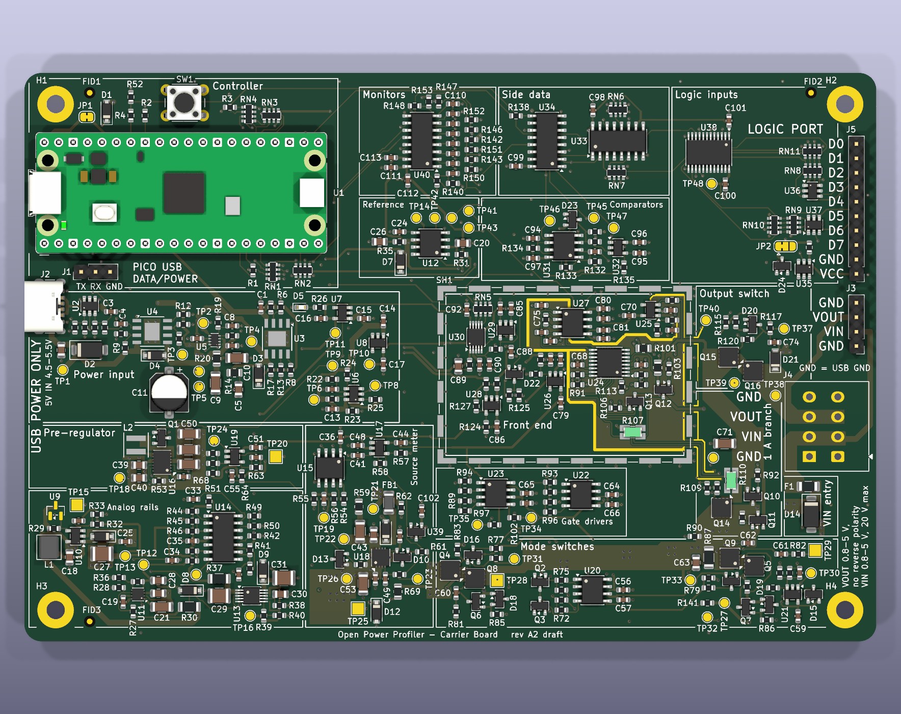
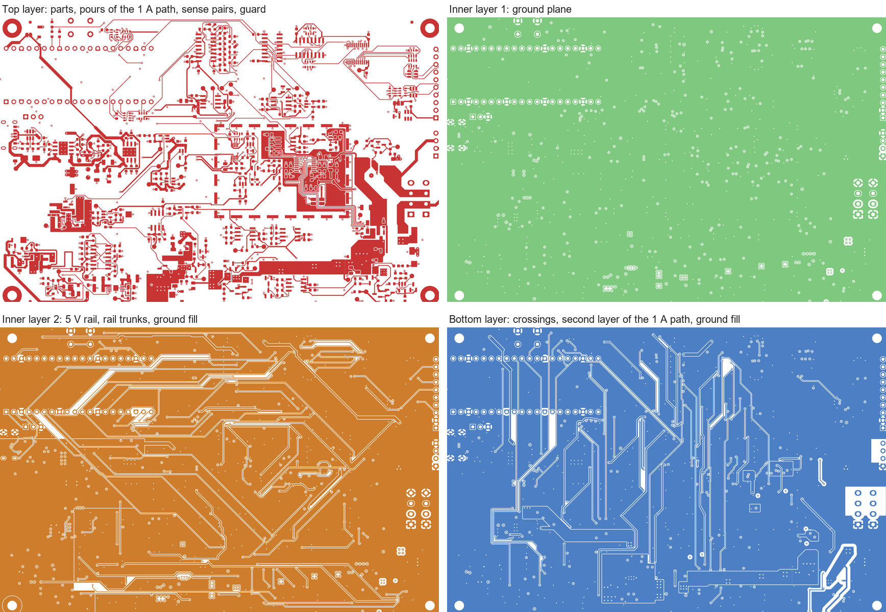
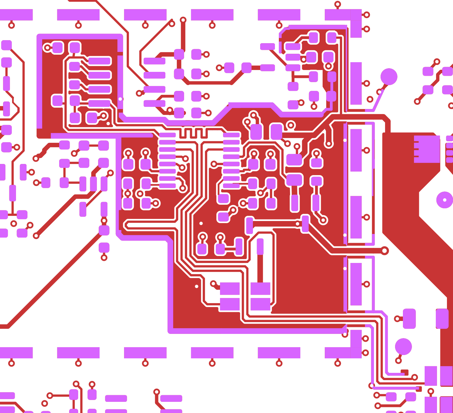
All pictures are renderings and plots of the board file, not photographs. The six pictures of the board were made again on 2026-10-13, from the board file after the round of that day: the two renderings and the plots of the copper layers, of the front end, of the 1 A path and of the placement.
The top side, rendered from the board file. The gold line around the front end is the guard under open solder mask, and the thin white frames with a name in each are the sixteen functional blocks as the silkscreen prints them:
The four copper layers side by side. Top left, the top layer: the parts, the pours of the 1 A path, the sense pairs and the guard. Top right, the first inner layer: the ground plane, in one piece. Bottom left, the second inner layer: the 5 V rail, the rail trunks and a ground fill. Bottom right, the bottom layer: the crossings, the second layer of the 1 A path and a ground fill:
The measured node under the shield can, top layer in red, openings of the solder mask in pink. Look for the pink line that runs around the large red area: it is the guard, bare of solder mask, around the copper of the measured node and the guard pour. From the multiplexer in the middle, thin lines run in pairs to the shunts: the Kelvin lines. At the lower right the pair of the 1 A range leaves the can in a lane with a guard track on each side:
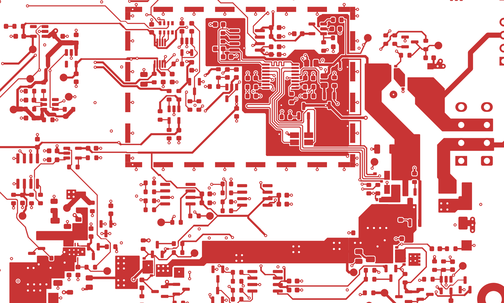
The 1 A path on the top layer. Follow the wide copper from the linear regulator at the bottom left, along the supply band to the right, up to the shunt branch and the output switch, and out to the terminal block at the right edge. The dashed rectangle is made of the lands of the shield can:
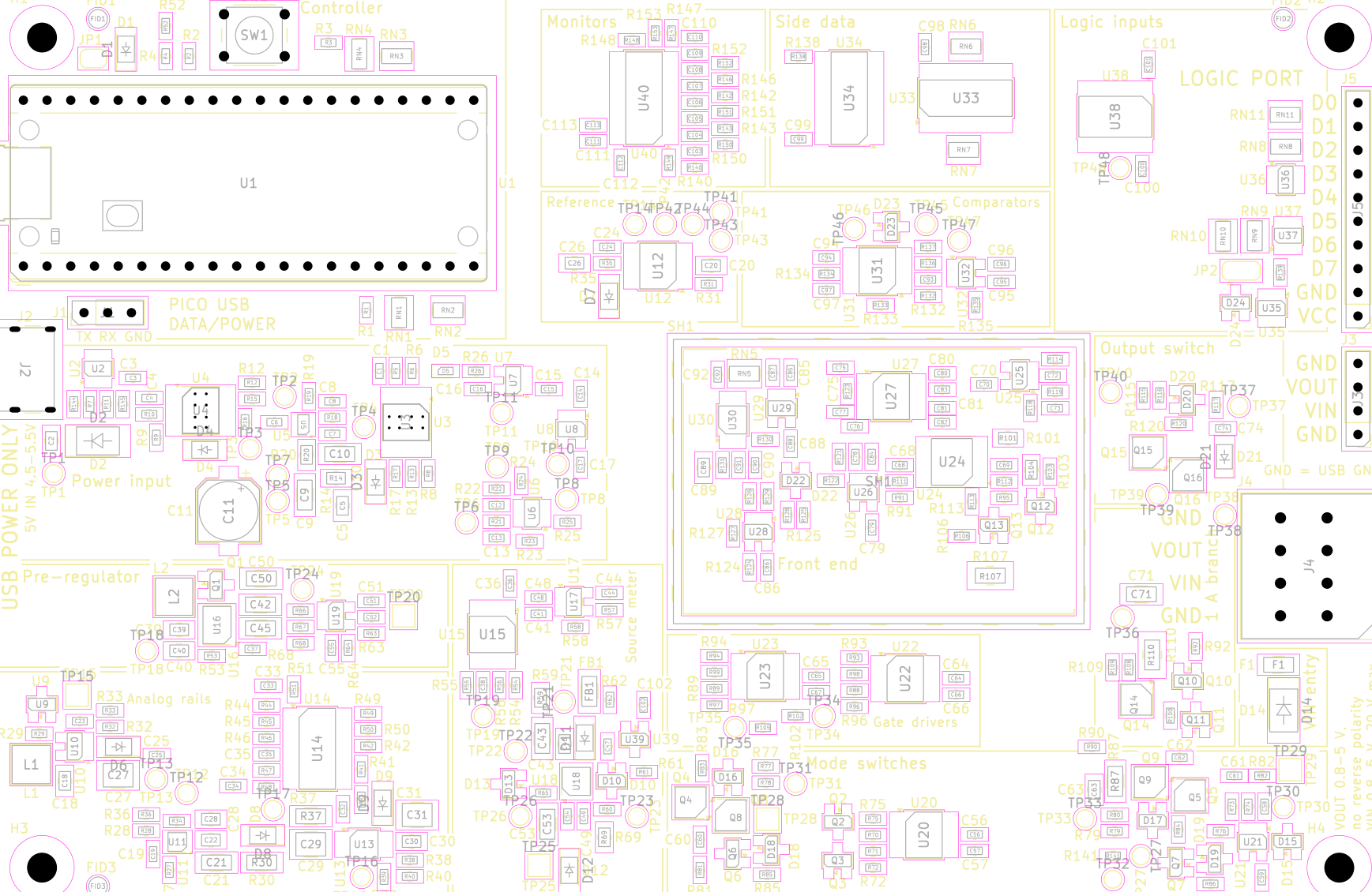
The areas of the sixteen functional blocks and the parts inside them. The plot shows the silkscreen with the frames and names of the blocks, the fabrication layer with the outlines and the references of the parts, and the courtyards:
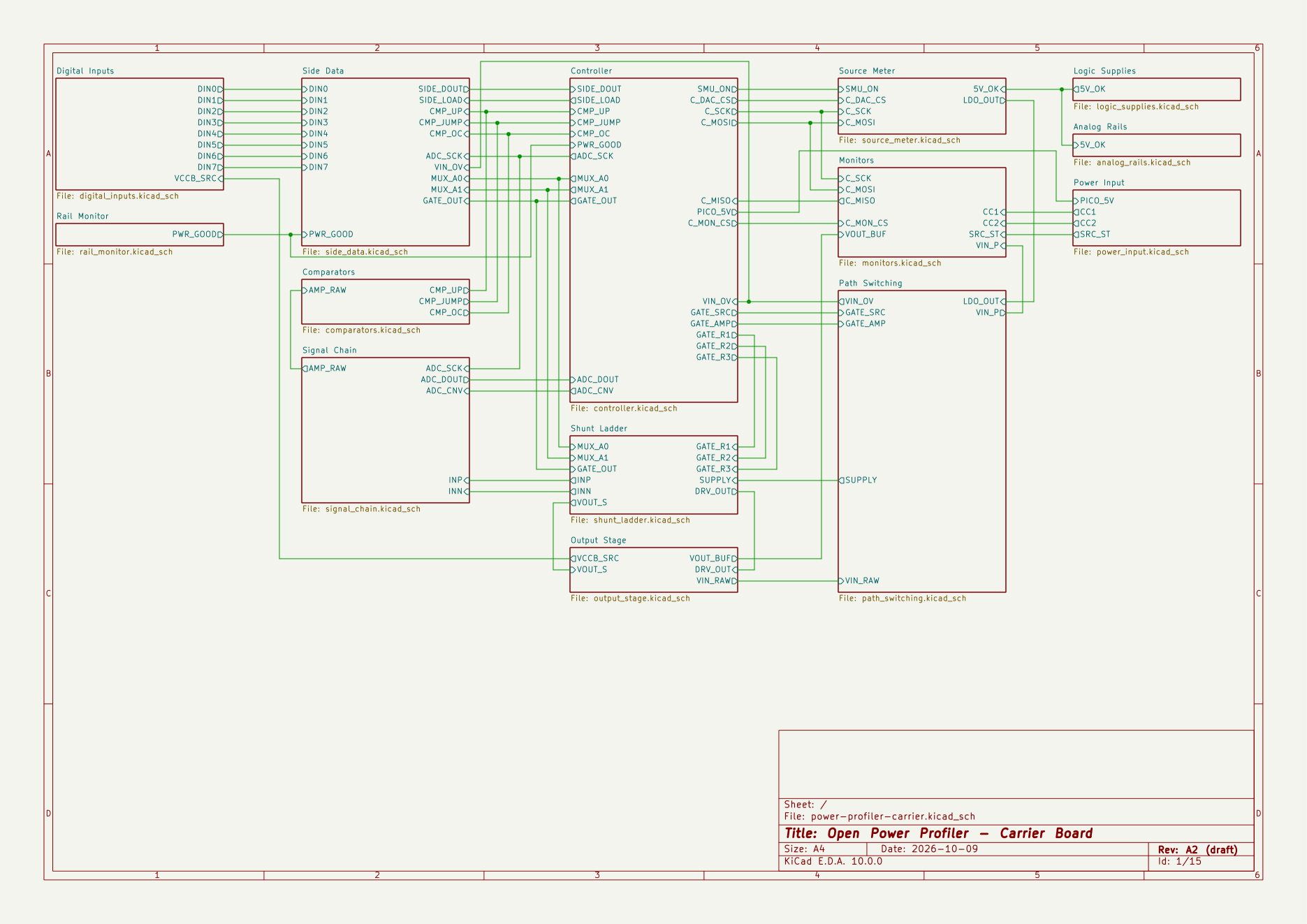
The root page of the schematic, with one block for each of the 14 sheets:
Every sheet and the board are shown in
hardware/doc/, and the whole schematic is in
hardware/doc/schematic.pdf. The status, the
checks and the open work are in the hardware guide.
The circuits of the carrier board are simulated from the netlist of the
schematic. A bench names parts of the schematic by their reference
designators, the package in simulation/ writes
their elements from a snapshot of that netlist, and ngspice runs the
circuit: no part of the board is typed by hand. What stands around the
parts is typed by the bench and named in its notes: sources, loads,
cables, and in some benches a stand-in for a neighboring block of the
board. The simulator is the ngspice library that KiCad 10 ships. Every
active part is a model written for this project from its datasheet, a
typical part at room temperature. 41 benches put these models into the
test circuits of their datasheets; four models have no such bench, the
analog multiplexer among them. The models of the manufacturers may not be
copied into the repository; where a copy is present they give a second
value.
Everything in this section is simulated. Nothing is built and nothing is measured: a figure that passes says that the simulated circuit keeps its limit with these models, not that a board will. Elsewhere on this page a figure marked "simulated" is one of the specification, taken from the earlier simulations of the draft.
The results are those of the run of 2026-10-10, on the circuit as it was drawn that day. Three decisions were drawn afterwards (D-95, D-97 and D-98), and the netlist snapshot of the package holds them since: 10 nF at the three capacitors of the rail monitor, the damper on the module input fitted, the new text of the detector position. The benches were not run again. Every figure below therefore comes from the circuit before these changes, with 1 nF at those capacitors and without the damper. Two cases that a bench set on purpose are the exception: one crossing of a rail with 10 nF, and the data cable plugged again with the damper. The benches of the power input still leave the two parts of the damper out. Bringing the benches in line with the snapshot and running the blocks that the changes touch, the rail monitor with the power-up and the power-off and the input from the module, is open work.
| Block | Benches | Pass | Fail | No limit |
|---|---|---|---|---|
| Shunt ladder | 2 | 20 | 0 | 6 |
| Signal chain | 11 | 113 | 8 | 111 |
| Range control logic | 12 | 143 | 6 | 122 |
| Source meter | 12 | 176 | 3 | 247 |
| Output stage | 6 | 151 | 6 | 142 |
| Path switching | 15 | 288 | 19 | 235 |
| Power input and logic supplies | 13 | 190 | 27 | 113 |
| Analog rails and rail monitor | 10 | 105 | 25 | 108 |
| Digital lines and monitors | 10 | 145 | 11 | 49 |
| Whole measuring path | 2 | 25 | 0 | 3 |
| Circuits of the board, ten blocks | 93 | 1356 | 105 | 1136 |
| Models against their datasheets | 41 | 478 | 17 | 70 |
| All | 134 | 1834 | 122 | 1206 |
A bench is one circuit with its stimulus. It takes figures from the waveforms and judges each one against its limit: a figure of the specification where it states one; else a rating or a figure of a datasheet, a value that the bench calculates, or a limit that the bench sets and names. For a model the limit is the figure of its datasheet with the tolerance that this project asks of a model. 1206 figures carry no limit: they are values that nothing limits. A figure that fails is kept as it is. Most of the 122 are of five kinds: a point that is decided since, whose figures are still those of the circuit before the decision, a figure of the specification that the circuit does not give, a rating that a fault case passes, an option that is not in use, and a model that misses its datasheet. The guide sorts them by block.
How close the simulated values lie: for 595 figures of the board blocks the pages print the distance from a stated value, in most cases the one that the specification states. 368 lie less than 5 % from it, 434 less than 10 % and 489 less than 25 %. The index of the results has every bench, and the page of each block has the values, the graphs and the decks, the circuit files that the simulator ran. The whole suite ran on one Windows machine and takes 29 minutes there.
Reproduced. The central design figures of the specification come out of circuits taken from the netlist. That is a second calculation with models, not a confirmation by measurement. Among them:
Four points, decided. The simulations raised them for a decision before boards are ordered, and the project owner decided them on 2026-10-10. Three are drawn since that day and one is not. The benches were not run again, so the results above are still those of the circuit before them:
Fourteen places where the simulation and the text differed. They were figures and rules of the specification, and things on which it was silent: how long the over-current comparator stays high while a large capacitor recharges, the ladder clamp in a short circuit, the advice on a capacitor at the VIN terminals, the times at power-off, the opening time of the output switch at 0.8 V, the current in the output suppressor at a trip, three figures of the mode switches, a check of section 16 that the simulation does not meet, the list of terms of the noise budget, the timing estimates of the converter lines, the leakage of the monitor converter, figures of the source meter, the in-rush on a computer port and the range that a logic input withstands. Twelve are corrected in the specification since 2026-10-10, each with the simulated figure. Three of the corrections are decisions: the over-current trip counts its time in the 1 A range only (D-99), the advice on a capacitor at the VIN terminals is limited to what was simulated (D-100), and the range of a logic input is stated as 0 V to 5.5 V (D-101). The times at power-off and the figures of the power input wait for the run of the benches on the drawn decisions. Seven questions stay open, each with one recommendation in section 16 of the specification. The fourteen are not every difference: the guide names the further figures that fail against a rating of a datasheet.
What stays for the bench. The simulations cannot settle the linear range of the amplifier near the negative rail, the loop of the pre-regulator at its low end, the linear regulator at light load, a supply that leaves its range while the path is closed, leakage at the nanoampere level, the programs of the controller, coupling through the board and temperature.
The simulation guide gives each of these with its figures, with the bench that shows it and with the limits of the models behind it.
Both pictures are plots of simulation runs, not measurements.
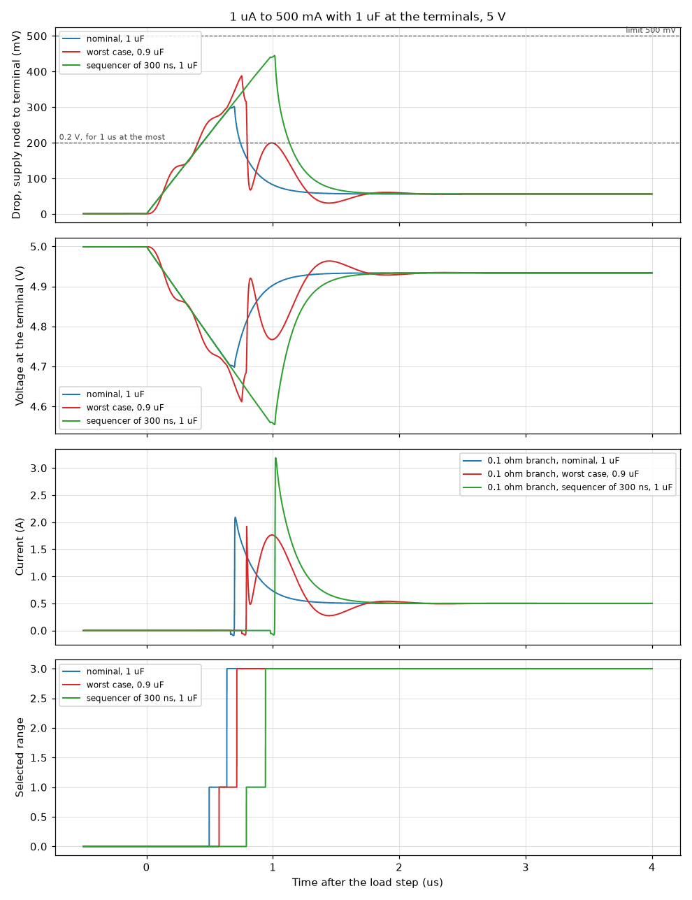
Requirement R-07 in a simulation. The load steps from 1 µA to 500 mA in the lowest range, with 1 µF at the terminals and 5 V at the output. From the top: the drop between the supply node and the output terminal, the voltage at the terminal, the current in the branch of the 0.1 Ω shunt, and the selected range. The step-up comparator takes the next range, then the jump comparator takes the path to the 1 A range. The drop peaks at 301.9 mV with nominal delays and at 388.2 mV with every delay at its limit and the capacitor 10 % low, against the limit of 500 mV. The requirement also allows the drop above 0.2 V for 1 µs at the most, which is the dashed line; the two curves are above it for 302 ns and 390 ns. The third curve gives the sequencer 300 ns, three times what the specification allows it, and reaches 445.1 mV. The reaction time of the sequencer is an input of this run: the program that has to keep it is not written.
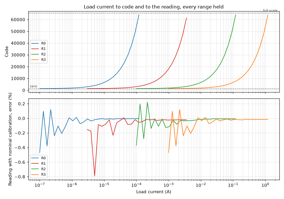
The whole measuring path in a simulation: ladder, multiplexer and amplifier chain as one circuit from the netlist, each range held while the load current rises to 120 % of its full scale. Above, the code of an ideal 16-bit converter at the converter input: the four ranges cover 100 nA to 1.2 A, with zero at code 1313. Below, the error of the reading with the nominal calibration against the load current; at small currents it is the rounding to one code. The amplifiers have no offset, no bias current and no noise in this run, and the converter is arithmetic.
| Path | Content | License |
|---|---|---|
firmware/ | Firmware of the controller: a project of the Pico SDK for the Pico 2, with a hardware-independent core and its unit tests; no adapter for the hardware and no PIO program yet | MIT; the helper cmake/pico_sdk_import.cmake is a copy from the Pico SDK and keeps the license in its header |
hardware/ | KiCad project of the carrier board, its pictures and bill of materials, and the fabrication outputs of draft A2: Gerber and drill files and two assembly files, filed for an order of proof-of-concept boards (D-105) | CERN-OHL-P v2 |
simulation/ | Circuit simulations of the carrier board: the package circuit-sim with its tests, a snapshot of the netlist of the schematic, the models written for the project, the benches and their results | MIT; the netlist snapshot in netlist/ and the results in results/: CERN-OHL-P v2 |
host/ | Python package: protocol, transports, device client, capture helpers, simulator | MIT |
protocol/ | Protocol definition, generator and shared test vectors | MIT |
tools/ | tools/board/: the package that calculates the layout figures from the board file, with its tests. The folders for the calibration and production-test scripts are empty | MIT |
docs/ | Specification, firmware design, component checks (all open), test reports (none yet) | MIT |
The work is split into phases. Each phase is closed by a test report with recorded measurements. The exit criteria are in section 13 of the specification.
| Phase | Goal | Status |
|---|---|---|
| 1 | Risk prototypes. On a Pico 2 with an ADC evaluation module: firmware on the Pico SDK, hardware-timed ADC capture, reaction time of the range sequencer, USB throughput. On evaluation modules: the pre-regulator with its tracking amplifier, and the start of the boost converter from a supply limited to 0.7 A | Not started: nothing has run on a Pico 2. Written ahead of it and tested without hardware: the firmware core, the protocol at version 2 and the host package. The firmware builds for the Pico 2 with the Pico SDK since 2026-10-12; the image has not been loaded onto a board, and what the phase measures is not written: the capture, the PIO programs and the USB link. The bench work is not started |
| 2 | Analog front end with one fixed range on a test board | Not started |
| 3 | Shunt ladder and range logic | Not started |
| 4 | Source mode and power | Not started |
| 5 | Carrier board, revision A, with the Pico 2 plugged in. Entry: the open checks that precede fabrication are closed and the layout is reviewed | Not started; draft A2 of the schematic and a board with every connection drawn exist, drawn ahead of the phases. The layout was reviewed with scripts and by calculation, and its seven deviations from section 10 are recorded decisions (D-87 to D-93). Of the four decisions that follow the simulations, three are drawn since 2026-10-10 (D-95, D-97 and D-98). On 2026-10-13 the project owner looked at the project in the KiCad editor and found it coherent, and the footprints and the placement were reviewed with scripts, 3D renderings and datasheets; the five findings of that review are worked into the board. Still to do: the fourth decision drawn (D-96), the benches that the drawn decisions touch run again, the review of the board item by item by a person in the KiCad editor, and the open items. The fabrication outputs of draft A2 are filed since 2026-10-13 for an order of proof-of-concept boards (D-105). Such boards are draft A2 and not revision A, and no order is recorded |
| 6 | Calibration, protocol freeze and host software | Not started |
| 7 | Revision B and release | Not started |
Draft A2 is the hypothesis that the phases test: the component checks and the results of phases 1 to 4 change it before revision A is fabricated. Proof-of-concept boards of the draft may be made before that: the project owner decided so on 2026-10-13, and the fabrication outputs are filed (D-105). Such boards are draft A2, not revision A. The circuit simulations test the same hypothesis ahead of the bench, with models in place of parts. They are not a phase and close none: a phase is closed by measurements. The work that comes first is listed under Project Status.
git clone https://github.com/Guiimartinho/open-power-profiler.git
cd open-power-profiler
Start with the specification. Each part of the repository documents its own setup and commands:
| Part | Needs | Guide |
|---|---|---|
| Firmware | CMake, Ninja and gcc for the unit tests; for the image of the Pico 2 also the Pico SDK 2.3.1 and the Arm GNU Toolchain | firmware/README.md |
| Host software | Python 3.10 or later | host/README.md |
| Protocol | Python 3.11 or later | protocol/README.md |
| Hardware | KiCad 10 | hardware/README.md |
| Board figures | Python 3.10 or later; KiCad 10 to dump the board file | tools/board/README.md |
| Circuit simulations | Python 3.10 or later; the ngspice shared library, which KiCad 10 ships | simulation/README.md |
| Documentation | Node.js, for npx --yes markdownlint-cli2@0.23.3 | CONTRIBUTING.md |
No instrument is needed to work on the software: the firmware logic runs in unit tests on the PC and its image builds without a board, the host package talks to a simulator, the board figures package is tested on small synthetic boards, and the circuit simulations need only the ngspice library that KiCad installs.
Firmware,
Host, Protocol, Tools, Simulation, Hardware, Docs), build
the firmware, run the tests with coverage floors, run the formatters and
static analyzers and check the hardware project. The firmware build is
the one for the Pico 2 since 2026-10-12: its job in the Firmware
workflow was rewritten for the Pico SDK and has not been started yet.
For now the workflows are started by hand, not on every push (D-22);
the same checks run locally before a change is recorded.tools/board/ has the gates of the host
software: tests with a coverage floor of 90 % of lines and branches,
ruff, mypy in strict mode, and the wheel built and installed. They ran
locally on Windows; the Tools workflow, which repeats them on Linux
and macOS too, has not been started yet.simulation/ has those gates as well: 777
tests, of which 11 need the ngspice library, ruff, and mypy in strict
mode over the package, its tests and the benches. Lines and branches
are covered in full against a floor of 90 %; the one module that loads
the simulator runs in a child process and is outside that measurement.
The gates ran locally on Windows with Python 3.11, last on 2026-10-12;
the Simulation workflow has not been started yet. They cover the
package, not the board: a figure that fails in a simulation breaks no
gate. It is a finding, and it is kept.The rules are in section 18 of the specification and in the contributing guide.
Contributions are welcome. Read the contributing guide first: it covers the workflow, the commit message format, the quality gates and how changes to the specification are recorded.
hardware/:
CERN-OHL-P v2.simulation/:
the snapshot of the netlist in simulation/netlist/ and the decks,
records, graphs and pages in simulation/results/, under the same
CERN-OHL-P v2, with a copy of the license in each of the two folders.esp32-s3-power-profiler
until its controller changed.| Qty | Value | Footprint | References |
|---|---|---|---|
| 51 | 100n 50V X7R | Capacitor_SMD:C_0603_1608Metric | C1, C13, C25, C100, C101, C102, C103, C104, C105, C106, C107, C108, C109, C110, C111, C113 +35 |
| 20 | 1k 1% | Resistor_SMD:R_0603_1608Metric | R4, R26, R53, R60, R62, R70, R72, R75, R88, R89, R93, R94, R111, R112, R118, R146 +4 |
| 20 | 1u 25V X7R | Capacitor_SMD:C_0603_1608Metric | C6, C7, C14, C15, C16, C17, C19, C24, C41, C47, C56, C62, C64, C65, C78, C112 +4 |
| 17 | 100k 1% | Resistor_SMD:R_0603_1608Metric | R17, R24, R27, R42, R50, R78, R80, R85, R86, R103, R106, R109, R115, R148, R149, R151 +1 |
| 13 | 10k 1% | Resistor_SMD:R_0603_1608Metric | R16, R19, R23, R25, R41, R54, R113, R114, R126, R144, R145, R150, R152 |
| 10 | BAV199 | Package_TO_SOT_SMD:SOT-23 | D10, D13, D15, D16, D17, D18, D19, D20, D22, D23 |
| 7 | 4.7u 25V X7R | Capacitor_SMD:C_0805_2012Metric | C2, C18, C20, C22, C28, C30, C63 |
| 7 | CSD17577Q3A | Package_SON:VSON-8_3.3x3.3mm_P0.65mm_NexFET | Q4, Q5, Q8, Q9, Q14, Q15, Q16 |
| 5 | 10R 1% | Resistor_SMD:R_0603_1608Metric | R31, R61, R108, R120, R129 |
| 5 | 1N5819HW | Diode_SMD:D_SOD-123 | D1, D3, D4, D11, D12 |
| 5 | 22R 1% | Resistor_SMD:R_0603_1608Metric | R77, R79, R92, R100, R130 |
| 5 | 22u 25V X5R | Capacitor_SMD:C_1206_3216Metric | C42, C43, C45, C50, C53 |
| 5 | GND | TestPoint:TestPoint_Pad_2.0x2.0mm | TP15, TP20, TP25, TP28, TP29 |
| 4 | 10n 50V C0G | Capacitor_SMD:C_0603_1608Metric | C32, C33, C34, C74 |
| 4 | 10u 25V X5R | Capacitor_SMD:C_0805_2012Metric | C5, C39, C40, C46 |
| 4 | 5.1k 1% | Resistor_SMD:R_0603_1608Metric | R7, R11, R91, R95 |
| 4 | B0530W 30V 0.5A | Diode_SMD:D_SOD-123 | D6, D7, D8, D9 |
| 4 | IRLML0030 | Package_TO_SOT_SMD:SOT-23 | Q10, Q11, Q12, Q13 |
| 4 | M3 | MountingHole:MountingHole_3.2mm_M3_Pad | H1, H2, H3, H4 |
| 4 | TPD4E1U06DBVR | Package_TO_SOT_SMD:SOT-23-6 | U2, U35, U36, U37 |
| 3 | 0.33R 1% | Resistor_SMD:R_0805_2012Metric | R14, R20, R59 |
| 3 | 100k 0.1% 25ppm | Resistor_SMD:R_0603_1608Metric | R36, R67, R74 |
| 3 | 10u 25V X7R | Capacitor_SMD:C_1210_3225Metric | C27, C29, C31 |
| 3 | 2.2M 1% | Resistor_SMD:R_0603_1608Metric | R83, R84, R117 |
| 3 | 22u 10V X7R | Capacitor_SMD:C_1206_3216Metric | C9, C10, C21 |
| 3 | 47R 1% | Resistor_SMD:R_0603_1608Metric | R102, R105, R119 |
| 3 | 49.9k 1% | Resistor_SMD:R_0603_1608Metric | R44, R46, R47 |
| 3 | 6.8k 1% | Resistor_SMD:R_0603_1608Metric | R52, R81, R82 |
| 3 | BSS138 | Package_TO_SOT_SMD:SOT-23 | Q1, Q2, Q3 |
| 3 | Fiducial | Fiducial:Fiducial_1mm_Mask2mm | FID1, FID2, FID3 |
| 3 | GND | TestPoint:TestPoint_Pad_D1.5mm | TP7, TP8, TP39 |
| 3 | OPA197IDBV | Package_TO_SOT_SMD:SOT-23-5 | U17, U25, U26 |
| 3 | OPA365AIDBV | Package_TO_SOT_SMD:SOT-23-5 | U19, U28, U29 |
| 3 | TC4427EOA | Package_SO:SOIC-8_3.9x4.9mm_P1.27mm | U20, U22, U23 |
| 2 | 1.5k 1% | Resistor_SMD:R_0603_1608Metric | R3, R51 |
| 2 | 100k | Resistor_SMD:R_Array_Convex_4x0603 | RN6, RN7 |
| 2 | 10k 0.1% 25ppm | Resistor_SMD:R_0603_1608Metric | R22, R57 |
| 2 | 11k 0.1% 25ppm | Resistor_SMD:R_0603_1608Metric | R58, R124 |
| 2 | 120k 1% | Resistor_SMD:R_0603_1608Metric | R140, R142 |
| 2 | 1k 0.1% 25ppm | Resistor_SMD:R_0603_1608Metric | R127, R137 |
| 2 | 1n 50V C0G | Capacitor_SMD:C_0603_1608Metric | C12, C58 |
| 2 | 2.00k 0.1% 25ppm | Resistor_SMD:R_0603_1608Metric | R55, R56 |
| 2 | 220p 50V C0G | Capacitor_SMD:C_0603_1608Metric | C23, C77 |
| 2 | 22p 50V C0G | Capacitor_SMD:C_0603_1608Metric | C75, C76 |
| 2 | 3.01k 1% | Resistor_SMD:R_0603_1608Metric | R6, R10 |
| 2 | 3.9k 1% | Resistor_SMD:R_0603_1608Metric | R125, R128 |
| 2 | 330R | Resistor_SMD:R_Array_Convex_4x0603 | RN8, RN9 |
| 2 | 4.53k 1% | Resistor_SMD:R_0603_1608Metric | R5, R9 |
| 2 | 4.7k | Resistor_SMD:R_Array_Convex_4x0603 | RN2, RN3 |
| 2 | 4.7k 1% | Resistor_SMD:R_0603_1608Metric | R1, R71 |
| 2 | 402k 1% | Resistor_SMD:R_0603_1608Metric | R8, R12 |
| 2 | 470k | Resistor_SMD:R_Array_Convex_4x0603 | RN10, RN11 |
| 2 | BC847B | Package_TO_SOT_SMD:SOT-23 | Q6, Q7 |
| 2 | LP5907MFX-3.3 | Package_TO_SOT_SMD:SOT-23-5 | U7, U8 |
| 2 | MCP6561T-E/OT | Package_TO_SOT_SMD:SOT-23-5 | U21, U32 |
| 2 | SN74LV165ADR | Package_SO:SOIC-16_3.9x9.9mm_P1.27mm | U33, U34 |
| 2 | TPS259621DDAR | Package_SO:TI_SO-PowerPAD-8_ThermalVias | U3, U4 |
| 1 | +12V_A | TestPoint:TestPoint_Pad_D1.5mm | TP16 |
| 1 | +13V5 | TestPoint:TestPoint_Pad_D1.5mm | TP13 |
| 1 | +3V3_A | TestPoint:TestPoint_Pad_D1.5mm | TP10 |
| 1 | +3V3_C | TestPoint:TestPoint_Pad_D1.5mm | TP11 |
| 1 | +5V | TestPoint:TestPoint_Pad_D1.5mm | TP6 |
| 1 | -4V_A | TestPoint:TestPoint_Pad_D1.5mm | TP12 |
| 1 | 0.1R 0.25% 50ppm | Resistor_SMD:R_Shunt_Ohmite_LVK12 | R110 |
| 1 | 0.22R 1% | Resistor_SMD:R_0603_1608Metric | R131 |
| 1 | 0.47R 1% 0.25W | Resistor_SMD:R_1206_3216Metric | R37 |
| 1 | 0.47R 1% 0.5W | Resistor_SMD:R_1206_3216Metric | R87 |
| 1 | 0R | Resistor_SMD:R_0603_1608Metric | R2 |
| 1 | 1.02k 0.1% 25ppm | Resistor_SMD:R_0603_1608Metric | R122 |
| 1 | 1.21k 1% | Resistor_SMD:R_0603_1608Metric | R13 |
| 1 | 1.3k 1% | Resistor_SMD:R_0805_2012Metric | R69 |
| 1 | 1.5n 50V C0G | Capacitor_SMD:C_0603_1608Metric | C85 |
| 1 | 1.5u 4.6A | Inductor_SMD:L_Coilcraft_XxL4020 | L2 |
| 1 | 100R 1% | Resistor_SMD:R_0603_1608Metric | R139 |
| 1 | 100n 50V C0G | Capacitor_SMD:C_1206_3216Metric | C71 |
| 1 | 10n 25V C0G | Capacitor_SMD:C_0603_1608Metric | C90 |
| 1 | 10p 50V C0G | Capacitor_SMD:C_0603_1608Metric | C52 |
| 1 | 10u 16V X7R | Capacitor_SMD:C_0805_2012Metric | C26 |
| 1 | 10u 3A | Inductor_SMD:L_Wuerth_MAPI-4030 | L1 |
| 1 | 115k 0.1% | Resistor_SMD:R_0603_1608Metric | R73 |
The 309 most common of 425 parts.

JitterCompany/debug-tools
Collection of useful utility PCBs for development purposes


xmyoot/guarded-ph-acquisition-module
Guarded pH analog front end: KiCad design, fabrication files, ESP32-S3 bring-up firmware and engineering review. Unbuilt prototype.


ChrisHayward-dev/SapphireKicad
See the LastProduction branch for the most current revision
It measures 150 × 100 mm and has 4 copper layers, 1.6 mm thick.
425 parts, built around the OPA197IDBV, OPA365AIDBV, TC4427EOA713 and TPD4E1U06DBVR. The full list of its parts is on this page, with links to each part's symbol and footprint where PCBKit's library has them.
From the Guiimartinho/open-power-profiler repository on GitHub, at the commit this page was made from: the board is hardware/kicad/power-profiler-carrier.kicad_pcb and its schematic hardware/kicad/analog_rails.kicad_sch. PCBKit opens the board in the browser, with nothing to install.
Its repository publishes it under the MIT licence: you may reuse it on that licence's terms (keep the author's notice, and for a copyleft licence share your changes alike).