2 layers73.7 × 38.1 mm

 grumat/glossy-msp43015
Glossy MSP430 - Embedded GDB Debugger for MSP430
STLinkForm is an open-source printed circuit board by grumat, from the grumat/glossy-msp430 repository on GitHub, published under the GPL-2.0 licence. It is a 2-layer board of 73.7 × 38.1 mm with 68 parts on 76 nets, routed with 812 tracks and 124 vias.
It is built around the STM32F103CBT6, 74LS125DC and AD8531ARTZ(UMW), with the SRV05-4, 74LVCH2T45DC and HT7833 among its other parts. Its parts include 28 capacitors, 14 resistors, 9 ICs, 5 connectors and 2 diodes. It belongs with the sensors and measurement boards and the STM32 and MSP430 boards of this library.


This prototype board replaces the STM32 Bluepill proto-board as a result of the chip crisis started on early 20's, which caused a overwhelming cases of STM32F103 clones and counterfeits.
This project is moving to more recent releases of the STM32 as there is barely a chance that the STM32F103 will ever get manufactured again. Or it may happen that very limited production batches will be sold at a premium price, for those searching for original parts.
For the development of the project we need access to the hardware pins and interfaces that realizes our project. So, one of the easiest way to go is the STM32 Blue and Black Pill prototyping board. This board is based on one of the two existing options: The STM32 BluePill and the STM32 BlackPill boards, easily found on eShops.
This prototype board offers the following advantages:
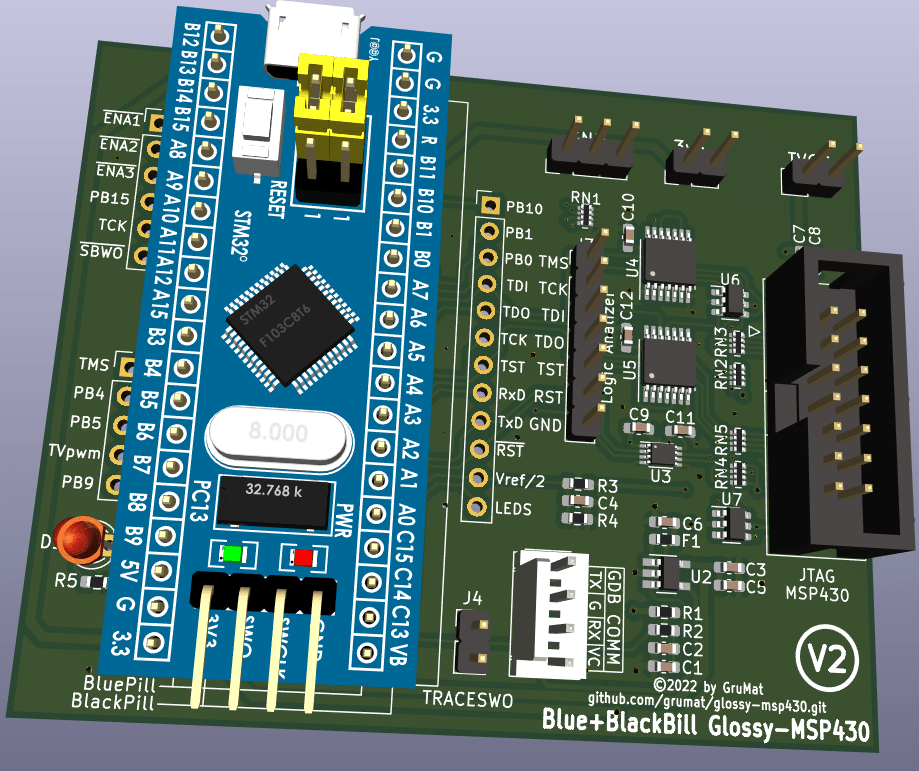
The BluePill/BlackPill prototype uses the following special features to implement the Glossy MSP430 device:
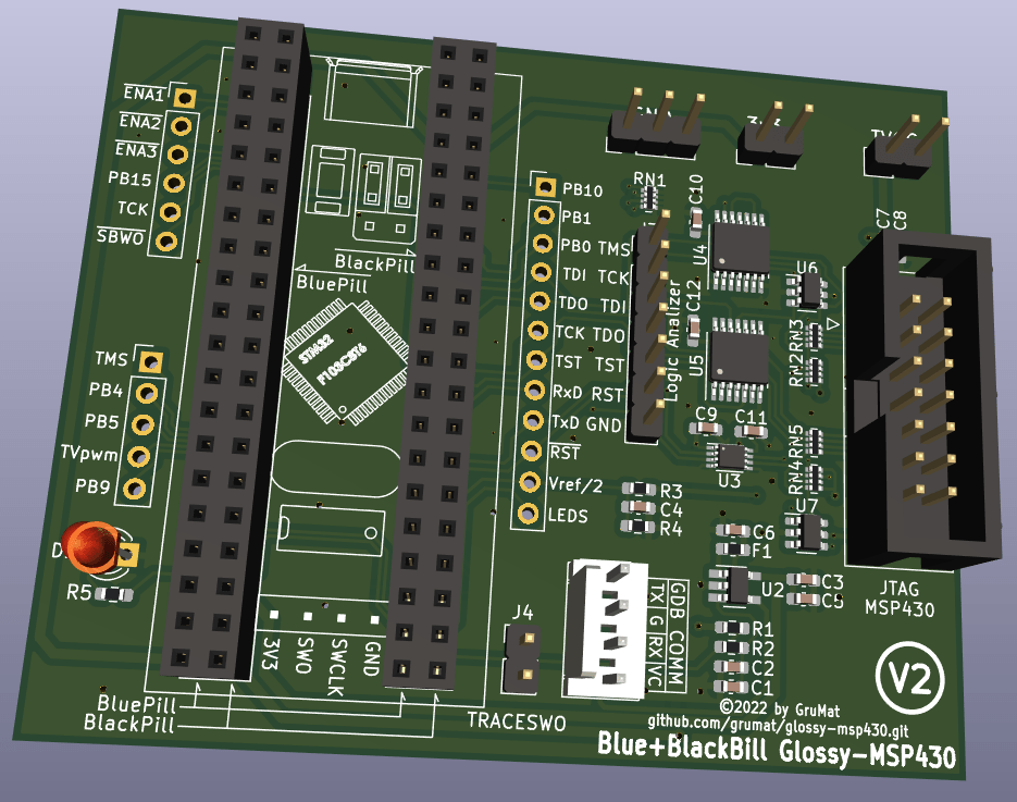
To allow for firmware debug capability on the early stage of development,
a GBD port is provided on USART1.
This is currently required, because when a device hosts a VCP, it is
required that the firmware is always online to react to USB host packets.
USB has a minimal flow of packets required for device management. But, a
minimal development framework needs the use of breakpoints. A breakpoint
will halt the CPU and cause a drop in the USB link because USB host will
stop receiving the minimal USB protocol frames. Therefore, a ordinary
USART is required for the step by step debugging.
Currently, the firmware found on the repository uses a stand-alone COM port hardware, so CPU flow may be stopped for debug inspection, while communication link is still online.
Note that the main impact of this combination is performance. Serial port will limit transfers to the serial line speed (bps). In the future, it is planned to implement an own VCP in the firmware, a huge performance gain will happen, because serial port packets on the USB side are essentially virtual and packets arrive directly on the USB payload buffers, no UART serialization is needed anymore. Payloads are handled directly in the firmware and bps won't cause any effect.
Transfer will follow these steps:
Quite promising!
Support for the older Bluepill board is also possible. For this option you should fit the board into the socket, aligned to the left row.
The detailed view can be seen on the following picture:
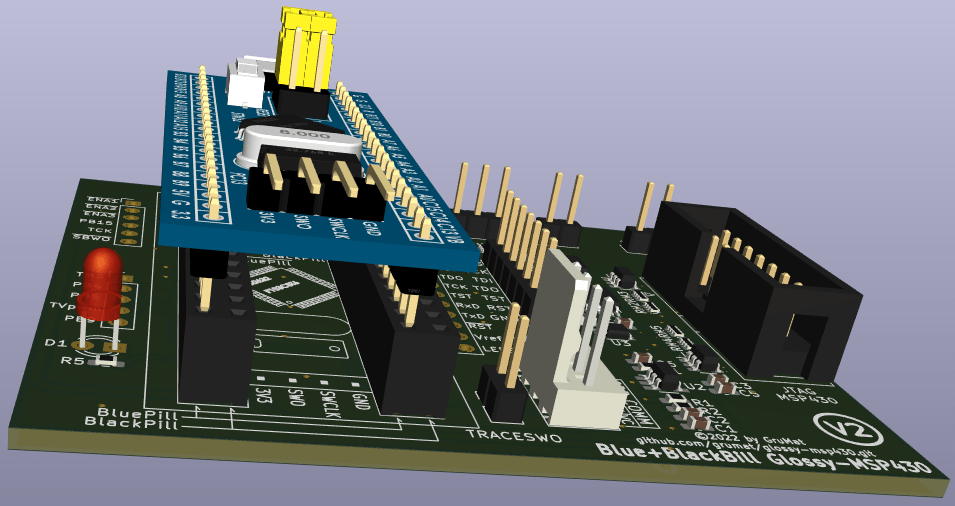
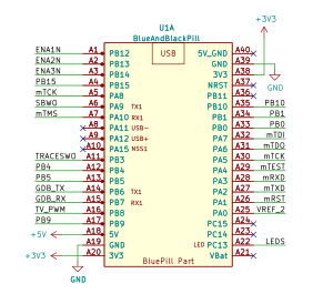
| Pin | Label | Description |
|---|---|---|
| PA0 | VREF_2 | ADC1 Ch0: Read target voltage samples |
| PB8 | TV_PWM | TIM4_CH3: PWM for DC voltage generator |
| Pin | Label | Description |
|---|---|---|
| PA1 | JRST | GPIO to control the JTAG RST line |
| PA4 | JTEST | GPIO to control the JTAG TEST line |
| PA5 | JTCK | SPI1_SCK to control the JTAG CLK line |
| PA6 | JTDO | SPI1_MISO to control the JTAG TDO line |
| PA7 | JTDI | SPI1_MOSI to control the JTAG TDI line |
| PA8 | JTCK_IN | TIM1_CH1 to sample JTAG clock |
| PA10 | JTMS | TIM1_CH3 to generate TMS waveform |
| Pin | Label | Description |
|---|---|---|
| PA9 | SBWO | Controls direction of SBW data line |
| PB12 | ENA1N | Control lines common to JTAG and SBW |
| PB13 | ENA2N | Control lines required by JTAG |
| PB14 | ENA3N | Control lines required by UART |
JTAG connector lines are negative logic signals and will have the following scenarios:
| SBWO | ENA1N | ENA2N | ENA3N | Function |
|---|---|---|---|---|
| 1 | 1 | 1 | 1 | HiZ; bus is disabled |
| 1 | 1 | 1 | 0 | UART active; Debug inactive |
| 1 | 0 | 1 | 0 | UART active; bus initialization |
| 1 | 0 | 0 | 0 | UART active; JTAG active |
| 0/1 | 1 | 0 | 0 | UART active; SBW active |
| 1 | 0 | 1 | 1 | UART inactive; bus initialization |
| 1 | 0 | 0 | 1 | UART inactive; JTAG active |
| 0/1 | 1 | 0 | 1 | UART inactive; SBW active |
| Pin | Label | Description |
|---|---|---|
| PA2 | JTXD | USART TXD line for target board |
| PA3 | JRXD | USART RXD line for target board |
| Pin | Label | Description |
|---|---|---|
| PA11 | USB_DM | USBD- signal of the USB device (onboard) |
| PA12 | USB_DP | USBD+ signal of the USB device (onboard) |
| Pin | Label | Description |
|---|---|---|
| PA13 | SWDIO | SWDIO signal in BluePill board |
| PA14 | SWCLK | SWCLK signal in BluePill board |
| PB3 | SWO | TRACE SWO signal for debug purpose |
| Pin | Label | Description |
|---|---|---|
| PB6 | GDB_TX | USART TXD line for GDB communication |
| PB7 | GDB_RX | USART RXD line for GDB communication |
| Pin | Label | Description |
|---|---|---|
| PB2 | BOOT0 | Bootloader (onboard) |
| PC13 | LEDS | Red (active low) and Green LED (active high) |
| Pin | Label | Description |
|---|---|---|
| PA15 | SYS_JTDI | Unused |
| PB0 | PB0 | Unused |
| PB1 | PB1 | Unused |
| PB4 | PB4 | Unused |
| PB5 | PB5 | Unused |
| PB9 | PB9 | Unused |
| PB10 | PB10 | Unused |
| PB11 | PB11 | Unused |
| PB15 | PB15 | Unused |
| PC14 | PC14 | Unused |
| PC15 | PC15 | Unused |
| VBAT | VBAT | Unused |
| NRST | NRST | Unused |
At the core of this prototype, a BlackPill development board is fitted into the main socket. Note that this socket uses dual row sockets, because it was designed to accommodate either a BlackPil or a BluePill board. The BlackPill should be fitted into the right pin row.
The detailed view can be seen on the picture below:
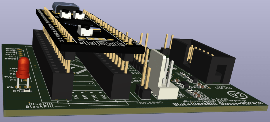
Please note that firmware development for the BlackPill is suspended because original STM32F411 have also disappeared since the chip crisis.
Worse than that, clones like the AT32F403 implements peripherals of the STM32F103 series, or a combo of both, which is counterproductive.
Newer STM32L4xx or STM32G4xx families are easier to buy and offers a substantial upgrade path.
The development of a big firmware is almost impossible without a tracing facility. SWO is the standard way to go. So this output has a dedicated access on the board, near to the SWD jumpers of the Blackpill (or Bluepill) board.
The Black Magic Probe provides an input pin for the SWO. Just connect a wire to the pin marked on that device.
Speeds of SWO may be an issue and experimentation proves that values listed on specs are far above the practical limits, when debugging and VCP is also handled simultaneously.
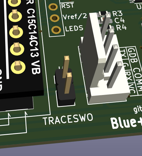
Note that on the final product, GDB connection is provided using a VCP
firmware implementation, which couples the tool at the max possible
transfer speed.
The advantage of the VCP firmware was covered on a topic above.
Regardless, a simple serial port is used during the core of the firmware
development.
Once the firmware is mature, the VCP will be added and this GDB serial
port will be deactivated.
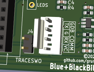
This connector can only be found on this prototype board. Final designs found on STLinkForm or StickForm does not incorporate this interface since they are planed when general firmware development gets more mature.
Two LEDs are provided to improve usability. One Red LED is already provided on the Blue/Black Pill board and a second, green colored, was added to the board.
Both LEDs share the same pin, like in a regular STLink. Either red or green, the color indicates the state of the JTAG bus and toggles during packet transfers coming from the host.
A red indicates that the JTAG bus is active (low impedance) and the green color indicates standby on a powered device.
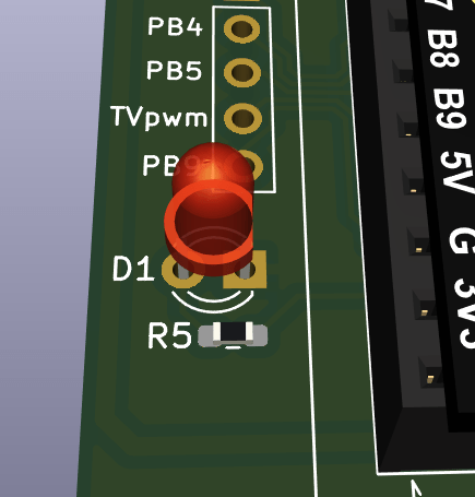
On the final design LEDs will se a component with dual LED integration, which is a more consistent solution than the one presented on this prototype board.
For a bus with a complex logic like the JTAG it is very important to check JTAG signals using a Logic Analyzer. So the board offers a dedicated connector for this purpose.
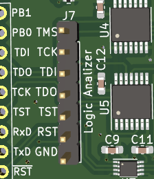
This connection is provided at the 3.3V realm, before the voltage translation occurs.
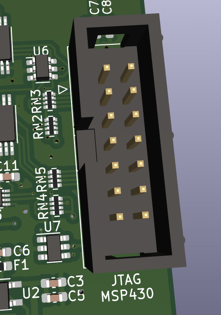
This is the connector used to connect the MSP430 board and follows the standard TI JTAG layout with additional pins for a serial VCP connection like proposed by Elprotronic.
Pins TDO, TDI, TMS, TCK, RST and TEST follows the same convention used by a standard MSP-FET, including both TDO and TCK which are also used for the Spy-bi-Wire connection.
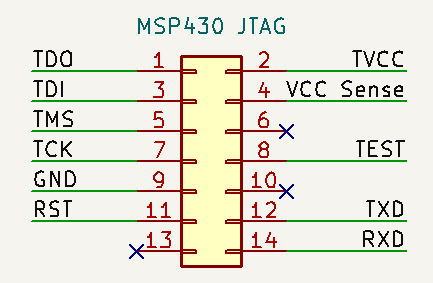
The MSP430 JTAG/BSL connectors from Elprotronic covers the fusion of JTAG and BSL into the same connector. At the end BSL uses a serial link, which is exactly appropriate for the VCP wiring. Note that like usual on a serial connection TXD and RXD interconnection needs to be crossed. So the pin 12 needs to be connected to a RXD pin on the MSP430, while the pin 14 will be tied to TXD pin on the target MCU (i.e. signal crossing occurs on the target board, not in this debug unit).
So for example, to establish a UART link to the USART0 of a classic MSP430F149 part, connect JTAG.12 to the P3.5/URXD0 and JTAG.14 to the P3.4/UTXD0 of the MCU.
Now for the Pin 2 TVCC line, this prototype board can supply up to
100 mA which is enough for almost every available daughter-board.
The VCC Sense pin is a reference entry for the cases that a board is
self powered. Then this reference voltage is used to adjust the TVCC
output voltage so that voltage levels are compatible.
Do not tie pins 2 and 4 together. They are mutually exclusive and official target boards implements a jumper for this selection (this rule is also valid when connecting a MSP430 to the official TI JTAG device).
Note that the Firmware can source a programmable voltage to the TVCC
line to supply the voltage translator circuit that can also be used to
attach a MSP430 target board using the JTAG connector.
This behavior is also seen on the official TI MSPFET and the older
MSPFET430UIF.
The TVCC supply voltage is protected by a 100 mA polyfuse, which should be enough for most practical cases.
A voltage translator was added to this test board, walking a step further if compared to the first BluePill prototype board, which allows for the development of the firmware coding that handles programmable supply voltages.
The output signal of this stage have ESD protection, which ensures that connecting cables to that connector is generally safe.
At the time of this writing, firmware still produces a fixed 3.3 V output on the TVCC line, which is used as reference for the target, even if hardware has support for variable voltage.
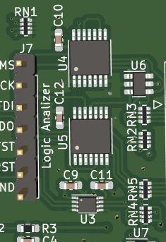
The circuit is based on a 74xx2T45 and two 74xx125. These circuits are capable of transferring signals at least at a 100 MHz rate, which is far more than the requirements for our application.
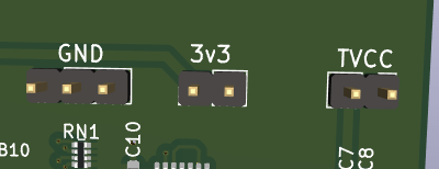
It is very often required to control supply voltages during firmware development, so the board has access to the GND, 3.3V and the TVCC.
Other interesting signals required for the implementation of the TVCC supply voltage are Vref and TVpwm, which are also accessible through the jumper pads around the BluePill/BlackPill.
The image below shows a typical use case of a firmware debug session:
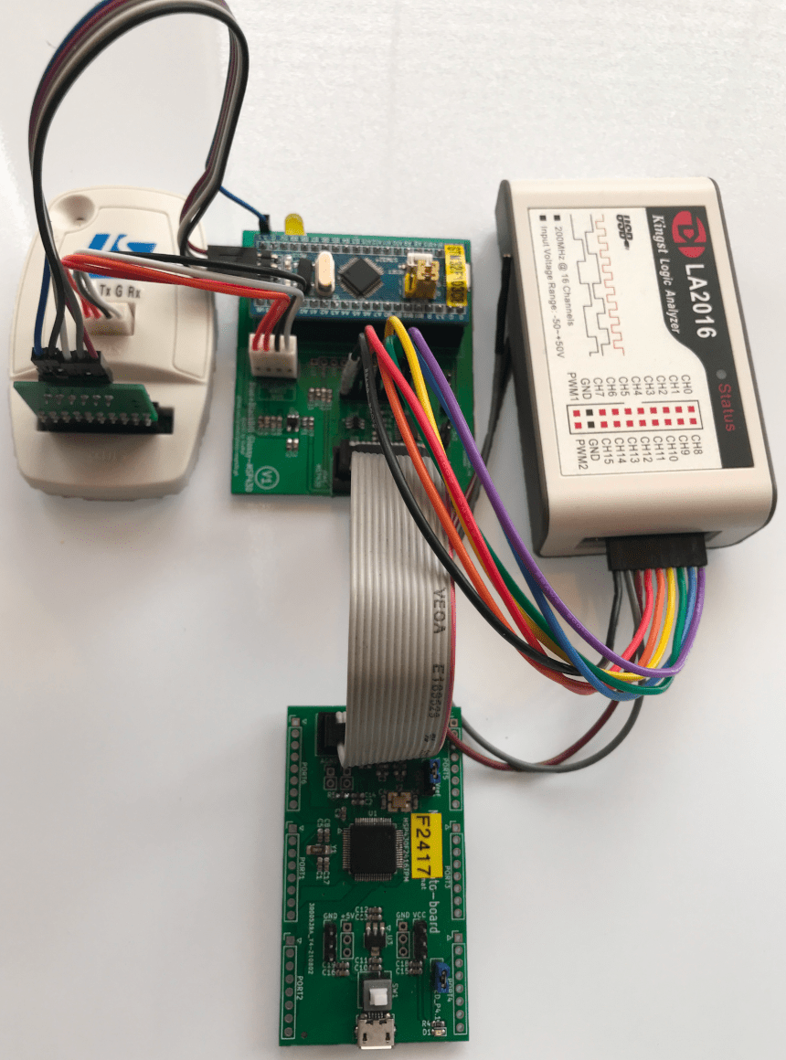
USB cable should be connected to the Black Magic Probe, the BluePill and the Logic Analyzer.
Each element of this picture are detailed next.
At the center you see the development board described on this topic.
In this setup a BluePill is seated at the dual connector. Connection cables are provided for the GDB UART port, the SWD debug port, TRACESWO, the Logic Analyzer and the MSP430 target board.
At the left you you see a STLink-clone converted to a Black Magic Probe (ARM) according to this article in our wiki.
In this particular conversion, the top connector, originally for the SWIM link, was converted to a 3.3V UART port. An internal hardware modification was required for this functionality and this port is used as the GDB debug port. Check the article.
Attached to the 20-pin ARM JTAG connector, an adapter board is used to
facilitate the wiring of the SWD+SWO connections. The output of this
adapter board has five wires running to the debug port of the
BluePill/BlackPill and the SWO jumper on the Development board.
Note that connection of the VCC supply is not advised, but here in
this image you will see that it has a wire, but although it cannot be
verified here, the adapter board has a switch to select the VCC
function.
Details to this SWD adapter board can be found on the hardware projects.
The logic analyzer in this picture is the LA2016 which has 16 inputs, but for this scenario only 6 inputs and the GND wire are required. All other cables are simply left unconnected.
An USB cable needs to be connected between the unit and the PC, so that the bundled software is able to capture signals.
The following image is an example of the 0x28 Shift IR command,
while the MSP board returns the 0x91 identification byte:
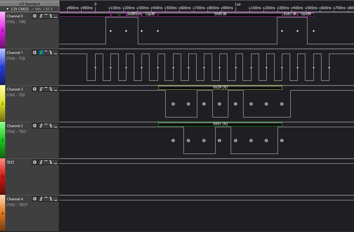
The SPI channel sends 3 bytes to perform this transmission, while the TMS signal was properly generated using a timer and DMA transactions. Since SPI requires byte aligned transfers we use TMS neutral states so that the some of the clock pulses have no effect on the payload.
On this repository you will find schematics and PCB for some MSP430 devices.
In this picture a MSP Proto Board is connected using a standard MSP430 14-pin flat cable. This uses the standard pinout for MSP430 JTAG emulators, also compatible with the commercial TI MSP-FET.
The particular device used in this case, is the MSP430F2417 and the target board is configured to use the 3.3V power supply provided by the BluePill board.
A brief documentation of the software development environment is described in here.
| Qty | Value | Footprint | References |
|---|---|---|---|
| 15 | 100nF | Capacitor_SMD:C_0603_1608Metric_Pad1.08x0.95mm_HandSolder | C3, C6, C8, C10, C11, C13, C15, C16, C17, C20, C21, C22, C25, C27, C28 |
| 5 | 10uF | Capacitor_SMD:C_0603_1608Metric_Pad1.08x0.95mm_HandSolder | C9, C14, C18, C23, C26 |
| 4 | 100K | Resistor_SMD:R_0603_1608Metric_Pad0.98x0.95mm_HandSolder | R1, R9, R10, R13 |
| 3 | 4k7 | Resistor_SMD:R_0603_1608Metric_Pad0.98x0.95mm_HandSolder | R3, R4, R14 |
| 3 | SRV05-4 | Package_TO_SOT_SMD:SOT-23-6 | U1, U7, U9 |
| 2 | 100 | lib:R_Array_Convex_4x0402_hand_soldered | RN1, RN2 |
| 2 | 12pF | Capacitor_SMD:C_0603_1608Metric_Pad1.08x0.95mm_HandSolder | C5, C7 |
| 2 | 1K | Resistor_SMD:R_0603_1608Metric_Pad0.98x0.95mm_HandSolder | R5, R8 |
| 2 | 20pF | Capacitor_SMD:C_0603_1608Metric_Pad1.08x0.95mm_HandSolder | C1, C4 |
| 2 | 22 | Resistor_SMD:R_0603_1608Metric_Pad0.98x0.95mm_HandSolder | R2, R7 |
| 2 | 22uF | Capacitor_SMD:C_0603_1608Metric_Pad1.08x0.95mm_HandSolder | C2, C19 |
| 2 | 330 | Resistor_SMD:R_0603_1608Metric_Pad0.98x0.95mm_HandSolder | R11, R12 |
| 2 | 47k | lib:R_Array_Convex_4x0402_hand_soldered | RN3, RN4 |
| 2 | 74LS125 | Package_SO:TSSOP-14_4.4x5mm_P0.65mm | U4, U5 |
| 2 | MountingHole | MountingHole:MountingHole_4mm | H1, H2 |
| 1 | 0 | NetTie:NetTie-2_SMD_Pad0.5mm | NT1 |
| 1 | 150141RV731 | LED_SMD:LED_Kingbright_AAA3528ESGCT | D2 |
| 1 | 1K5 | Resistor_SMD:R_0603_1608Metric_Pad0.98x0.95mm_HandSolder | R6 |
| 1 | 1k8 | Inductor_SMD:L_0603_1608Metric_Pad1.05x0.95mm_HandSolder | L1 |
| 1 | 1nF | Capacitor_SMD:C_0603_1608Metric_Pad1.08x0.95mm_HandSolder | C24 |
| 1 | 470nF | Capacitor_SMD:C_0603_1608Metric_Pad1.08x0.95mm_HandSolder | C12 |
| 1 | 74LVCH2T45DC | Package_SO:VSSOP-8_2.3x2mm_P0.5mm | U8 |
| 1 | 8MHz | Crystal:Crystal_SMD_3225-4Pin_3.2x2.5mm | Y1 |
| 1 | AD8531ARTZ | Package_TO_SOT_SMD:TSOT-23-5 | U6 |
| 1 | HT7833 | Package_TO_SOT_SMD:SOT-89-3 | U3 |
| 1 | ISP | Connector_PinHeader_2.54mm:PinHeader_1x04_P2.54mm_Vertical | J4 |
| 1 | JTAG | Connector_PinHeader_2.54mm:PinHeader_2x07_P2.54mm_Vertical | J2 |
| 1 | PMEG4010BEA,115 | Diode_SMD:D_SOD-323_HandSoldering | D1 |
| 1 | Polyfuse | Fuse:Fuse_0603_1608Metric_Pad1.05x0.95mm_HandSolder | F1 |
| 1 | RS232 | Connector_Molex:Molex_KK-254_AE-6410-04A_1x04_P2.54mm_Vertical | J3 |
| 1 | STM32F103CBT6 | Package_QFP:LQFP-48_7x7mm_P0.5mm | U2 |
| 1 | SWD | lib:PinHeader_2x05_P1.27mm_Vertical_SMD_case | J5 |
| 1 | USB_B_Micro | lib:USB_Micro-B_Molex-105017-0001-handsolder | J1 |


georges-mars/Docimeter
A wearable redesign of the OpenDosimeter platform focused on compact electronics, custom PCB integration, embedded firmware, and practical radiation-monitoring applications.


mornepousse/Niphargus
Niphargus — a slim, indestructible wireless split keyboard. ESP32 + nRF24, wired fallback, and an emergency kit hidden behind the USB port. The successor to the Rouge-Gorge.

AllenNeuralDynamics/harp.device.lickety-split
0360: an ephys-compliant capacitive lick detector

AllenNeuralDynamics/harp.device.treadmill-driver
0326: a Harp-compatible device for controlling an instrumented mouse treadmill

AllenNeuralDynamics/harp.device.sniff-detector
0382: Signal conditioning board for an implanted thermistor
It measures 73.7 × 38.1 mm and has 2 copper layers, 1.6 mm thick.
68 parts, built around the STM32F103CBT6, 74LS125DC, AD8531ARTZ(UMW) and SRV05-4. The full list of its parts is on this page, with links to each part's symbol and footprint where PCBKit's library has them.
From the grumat/glossy-msp430 repository on GitHub, at the commit this page was made from: the board is Hardware/STLinkForm/STLinkForm.kicad_pcb and its schematic Hardware/BlackPill-BMP/BlackPill-BMP.kicad_sch. PCBKit opens the board in the browser, with nothing to install.
Its repository publishes it under the GPL-2.0 licence: you may reuse it on that licence's terms (keep the author's notice, and for a copyleft licence share your changes alike).