
4 layers64.8 × 62.7 mm
 fstp/computer_clock_module
The clock module for my PCB computer
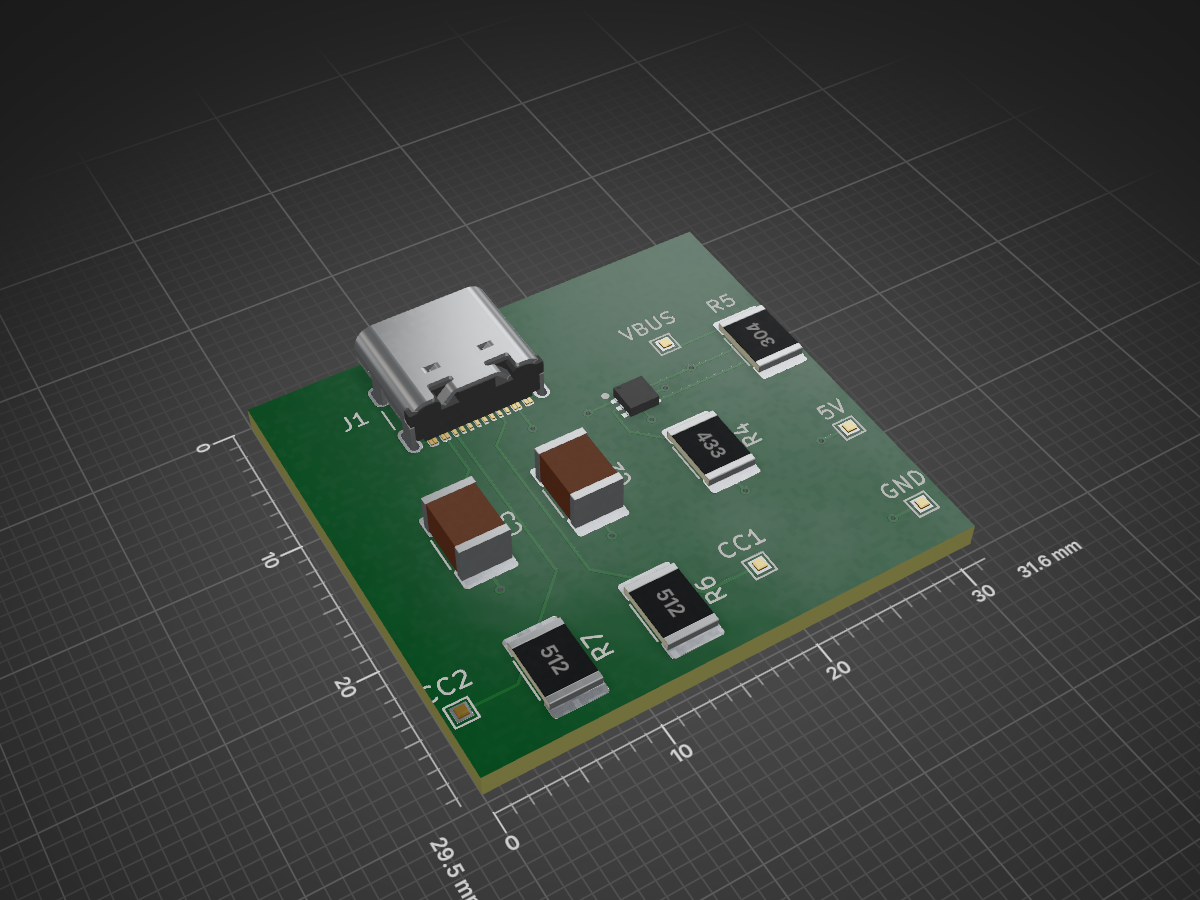
Usbc data is an open-source printed circuit board by fstp, from the fstp/computer_clock_module repository on GitHub. It is a 2-layer board with 13 parts on 13 nets, routed with 52 tracks and 11 vias.
It is built around the TPS25200DRVR. Its parts include 4 resistors, 2 capacitors, 1 IC and 1 connector. It belongs with the lEDs and displays boards of this library.
A dedicated PCB implementation of the clock module for a discrete 8-bit computer. This project is heavily inspired by Ben Eater's 8-bit computer series but adapts the breadboard schematics into a permanent, reliable Printed Circuit Board form factor. The clock module is the heartbeat of the computer. It synchronizes all operations across the bus, registers, and memory. This PCB module is designed to be modular, allowing it to be plugged into a larger backplane or connected via jumper wires to other components.
The circuit is built around the versatile 555 Timer IC. The design uses three distinct timers to handle signal generation and logic control:
The PCB exposes the following header pins:
| Name | Description |
|---|---|
| 5V_OUT | +5V supply output. |
| CLOCK_OUT | The clock output signal. |
| HALT_IN | The input halt signal. |
| GND_OUT | Ground supply output. |

Ben Eater: For the incredible 8-bit computer tutorial series which served as the primary inspiration for this project.| Qty | Value | Footprint | References |
|---|---|---|---|
| 2 | 5.1k | Resistor_SMD:R_1812_4532Metric_Pad1.30x3.40mm_HandSolder | R6, R7 |
| 1 | 0.1u | Capacitor_SMD:C_1812_4532Metric_Pad1.57x3.40mm_HandSolder | C3 |
| 1 | 22u | Capacitor_SMD:C_1812_4532Metric_Pad1.57x3.40mm_HandSolder | C2 |
| 1 | 300k | Resistor_SMD:R_1812_4532Metric_Pad1.30x3.40mm_HandSolder | R5 |
| 1 | 43k | Resistor_SMD:R_1812_4532Metric_Pad1.30x3.40mm_HandSolder | R4 |
| 1 | 5V | TestPoint:TestPoint_Pad_1.0x1.0mm | TP1 |
| 1 | CC1 | TestPoint:TestPoint_Pad_1.0x1.0mm | TP3 |
| 1 | CC2 | TestPoint:TestPoint_Pad_1.0x1.0mm | TP2 |
| 1 | GND | TestPoint:TestPoint_Pad_1.0x1.0mm | TP4 |
| 1 | TPS25200DRVR | SamacSys_Parts:SON65P200X200X80-7N | IC1 |
| 1 | USB_C_Receptacle_USB2.0_16P | Connector_USB:USB_C_Receptacle_GCT_USB4105-xx-A_16P_TopMnt_Horizontal | J1 |
| 1 | VBUS | TestPoint:TestPoint_Pad_1.0x1.0mm | TP5 |
13 parts, built around the TPS25200DRVR. The full list of its parts is on this page, with links to each part's symbol and footprint where PCBKit's library has them.
From the fstp/computer_clock_module repository on GitHub, at the commit this page was made from: the board is usbc_data.kicad_pcb and its schematic clock_module.kicad_sch. PCBKit opens the board in the browser, with nothing to install.
Its repository states no licence, so its author keeps all rights: ask fstp before reusing the design.

Student-Satellite-IITB/Communication-Subsystem
Communication Subsystem for IITBSSP CubeSat Mission


taskx6004/limejig
Open-source LimeJig fixture firmware, host tools, KiCad source, and synthetic test examples

deadbandlabs/syncro-mainboard
Hardware Design for Syncro FFB Interceptor


icarofcb/3.3V-Car-Voltage-Regulator-Grade-board
3.3V Car Voltage Regulator Grade board hardware

