Skip to the content
PCBKitNew board
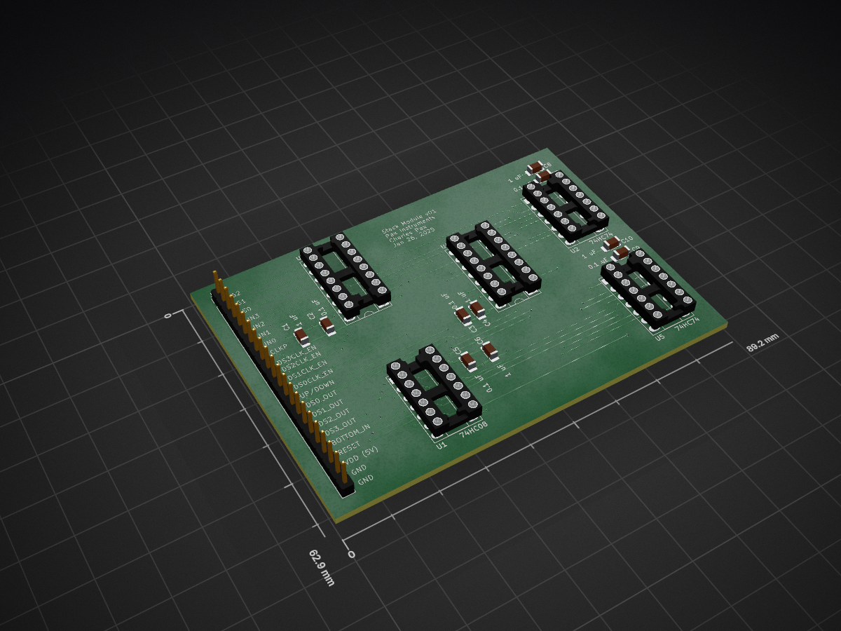
2 layers89.2 × 62.9 mmStack module, the printed circuit board in 3D

A project to create a microprocessor optimized for human visual verification

Size
89.2 × 62.9 mm
Copper layers
2
Thickness
1.6 mm
Parts
16
Nets
35
Pads
116
Tracks, vias
242, 71
Pours
1
Routed
Yes
KiCad
KiCad 8.0 (file 20240108)
Created
20 Dec 2022
Updated
1 Dec 2025

Overview

Stack module is an open-source printed circuit board by charlespax, from the charlespax/macroprocessor repository on GitHub, published under the MIT licence. It is a 2-layer board of 89.2 × 62.9 mm with 16 parts on 35 nets, routed with 242 tracks and 71 vias.

It is built around the 74HC74D, 74HC08D and 74HC151D, with the 74HC157D among its other parts. Its parts include 10 capacitors, 5 ICs and 1 connector.

Main components

4

README

README.md

macroprocessor

A project to create a microprocessor optimized for human visual verification

Introduction

A user should be able to trust the output of a computational device without having to trust the computatoinal device itself.

Application

Cryptographic security

Bitcoin

Design

The design is not optimized for price, area, power, efficiency, yield, or other traditional parameter. The design is optimized for human readability and understanding.

Requirements

  • MUST be visible to a human with minimal optical magnification
  • An integrated circuit design layout SHOULD aid understanding
  • IC layout SHOULD correspond to the layout as seen in a digitial simulation
  • Microprocessor design architecture SHOULD be optimized for understanding
  • The registers or other circuitry MAY emit light
  • MAY have features to aid cryptography
  • MAY have serial output for debugging or other purposes

Design notes

The overall chip layout and data flow SHOULD run from left to right.

Logical elements SHOULD have inputs on the left and outputs on the right

The metal layer or other features MUST NOT obscure any features such that the circuit can not be verified visually.

Chip packaging MUST NOT obscure the electrical path from the IC to the package pins.

The design MAY use multiple IC components if each component meets the requirements of this document.

The design MAY include wire-bonded components

Notes

  • RISC-V RV32I or RV32E are candidates
  • Research making a Forth-native processor
  • Can the macroprocessor be made using the same process as LEDs?
  • Can a wafer be put through a secondary LED process to create registers that emit light?
  • What is the current state of light-emitting transistors (LETs)?
  • Can I use diode logic and use LEDs?
  • I believe the normal silicon process cannot be used to create features that emit light because the band gap of silicon is too greaet. True?
  • RISC-V would be a great choice if it can be visually verified. This has the advantage that many more eyes would be on the chip. However, I think it is more important to make choices that result in more users in verifying their own devices.
  • Check out https://zeroToASICCourse.com - this is a course for designing and ordering your own chip designs.
  • Check out https://developers.google.com/silicon - Google's wafer batching program for open source designs. Cool, but I am happy to pay if reasonable.
  • MAY take an external diode-based ROM
  • Is there anything about this processor that would make it bad at cryptographic functions? Minimal circuitry could be included to address issues.
  • Can x-ray crystalography be used to verify the surface of an IC?
  • https://www.skywatertechnology.com is a US-based silicon fab.
  • What happens to the equipment from old semiconductor fabrication technologies?
  • Fab technologies: https://en.wikipedia.org/wiki/Semiconductor\_device\_fabrication
  • Are there fabs that use old technologies for new chips?
  • Wire bonding can be used in places where the metal layer would obscure layers below
  • wire bonding can be used as jumpers that can be cut to permanently disable a ffeature
  • Rather than wire bonding, the connections can be routed to the outside of the package, so they can be explicetly enabled
  • Maybe multi gate transistors can be used on such large features if one large gate is not appropriate
  • Make the binary instruction decoding physicallyl easy to see on the die. Put them in the same order you would find them in a specification table
  • Is silicon transparent to any frequency of light? If so, maybe this can be used for verification and would be a design consideration.

Conventions

The keywords below are to be interpreted as described in BCP14 [RFC2119] [RFC8174].

  • MUST
  • MUST NOT
  • REQUIRED
  • SHOULD
  • SHOULD NOT
  • RECOMMENDED
  • NOT RECOMMENDED
  • MAY
  • OPTIONAL

Parts

16
QtyValueFootprintReferences
50.1 uFCapacitor_SMD:C_1206_3216Metric_Pad1.33x1.80mm_HandSolderC2, C3, C5, C7, C9
51 uFCapacitor_SMD:C_1206_3216Metric_Pad1.33x1.80mm_HandSolderC1, C4, C6, C8, C10
274HC74Package_DIP:DIP-14_W7.62mm_Socket_LongPadsU2, U5
174HC08Package_DIP:DIP-14_W7.62mm_Socket_LongPadsU1
174HC151Package_DIP:DIP-16_W7.62mm_Socket_LongPadsU3
174HC157Package_DIP:DIP-16_W7.62mm_Socket_LongPadsU4
1Conn_01x22_PinConnector_PinHeader_2.54mm:PinHeader_1x22_P2.54mm_VerticalJ22

Questions

How big is the Stack module PCB?

It measures 89.2 × 62.9 mm and has 2 copper layers, 1.6 mm thick.

What parts does the Stack module use?

16 parts, built around the 74HC74D, 74HC08D, 74HC151D and 74HC157D. The full list of its parts is on this page, with links to each part's symbol and footprint where PCBKit's library has them.

Where can I download the Stack module KiCad files?

From the charlespax/macroprocessor repository on GitHub, at the commit this page was made from: the board is vm-digital/stack module/stack module.kicad_pcb and its schematic vm-digital/diode-matrix-rom-dip/diode-matrix-rom-dip.kicad_sch. PCBKit opens the board in the browser, with nothing to install.

Can I use the Stack module design in my own project?

Its repository publishes it under the MIT licence: you may reuse it on that licence's terms (keep the author's notice, and for a copyleft licence share your changes alike).

More from charlespax/macroprocessor

4
  • 2 layersDiode matrix rom, the printed circuit board in 3D

    Diode matrix rom

    charlespax/macroprocessor

    A project to create a microprocessor optimized for human visual verification

    31 partsMIT
  • 4 layers27.9 × 58.4 mmDiode matrix rom dip, the printed circuit board in 3D

    Diode matrix rom dip

    charlespax/macroprocessor

    A project to create a microprocessor optimized for human visual verification

    29 partsMIT
  • 2 layers14 × 30.1 mmStack DIP, the printed circuit board in 3D

    Stack DIP

    charlespax/macroprocessor

    A project to create a microprocessor optimized for human visual verification

    17 partsMIT
  • 4 layers27.9 × 45.7 mmTemp kicad, the printed circuit board in 3D

    Temp kicad

    charlespax/macroprocessor

    A project to create a microprocessor optimized for human visual verification

    15 partsMIT

Similar boards

  • 2 layers178 × 711 mmMSAP-2 rev.A SMD, the printed circuit board in 3D

    MSAP-2 rev.A SMD

    mehrantsi/MSAP-2

    An 8-bit computer. Successor to MSAP-1

    658 parts13MIT
  • 2 layers297 × 210 mmCpu, the printed circuit board in 3D

    Cpu

    tetrix450/masic-cpu

    MASIC CPU schematics and PCB

    197 partsMIT
  • 4 layers281 × 142 mmTuring Machine, the printed circuit board in 3D

    Turing Machine

    MelonMars/TuringPCB

    A Turing Machine that does not use any premade microchips, but rather is built exclusively on simple components.

    255 parts
  • 2 layers100 × 100 mmPortcard RevC, the printed circuit board in 3D

    Portcard RevC

    retrac0/retelex

    Retro telephone exchange. Also retro telex exchange.

    75 parts
  • 6 layers150 × 60 mmLogic macropad, the printed circuit board in 3D

    Logic macropad

    Greentalinjo/74HController

    A game controller built entirely from discrete 74HC logic - no microcontroller, a diode ROM and an 8-N-1 serial frame out of an RJ45 console port.

    170 parts
  • 4 layers177 × 152.1 mmAvboard tht2, the printed circuit board in 3D

    Avboard tht2

    clydeshaffer/gametank

    design files for the gametank hardware implementation

    139 parts150
  • 2 layers216 × 150 mmMotherboard-101, the printed circuit board in 3D

    Motherboard-101

    artemisamsx/artemisa

    Schematics, PCB designs and HDL simulations to build a 8-bits MSX computer

    124 parts67
  • 2 layers335 × 218.6 mmMSX Goauld, the printed circuit board in 3D

    MSX Goauld

    leomanes/stargate

    Stargate MSX Compatible Computer

    298 parts18GPL-3.0