4 layers91 × 53.1 mm
Nff pcb
o7-machinehum/flipper-blackhat
Linux based WiFi pentesting device for the Flipper Zero.
184 parts300

 Greentalinjo/74HController
A game controller built entirely from discrete 74HC logic - no microcontroller, a diode ROM and an 8-N-1 serial frame out of an RJ45 console port.
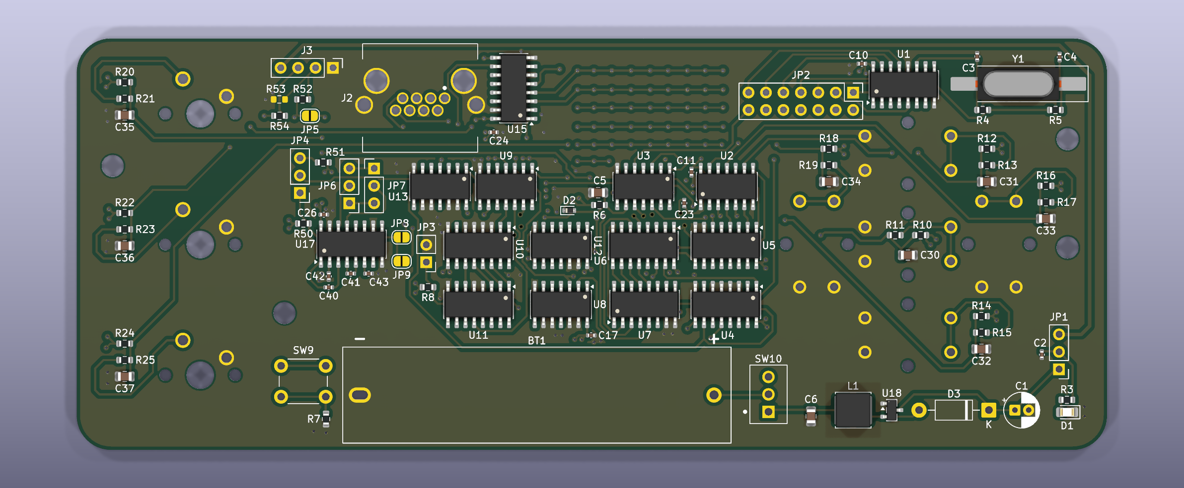
Logic macropad is an open-source printed circuit board by Greentalinjo, from the Greentalinjo/74HController repository on GitHub. It is a 6-layer board of 150 × 60 mm with 170 parts on 141 nets, routed with 1,482 tracks and 287 vias.
It is built around the MAX3232CSE+, ME2108A33M3G and 74HC14D, with the 74HC151D, 74HC161D and 74HC165D among its other parts. Its parts include 59 diodes, 35 capacitors, 34 resistors, 18 ICs and 6 switches. It belongs with the keyboards and input and interfaces and adapters boards of this library.


A game controller built entirely from discrete 74HC logic. Eight keys, a diode ROM for a character table, and a real 8-N-1 serial frame out of an RJ45 console port — no microcontroller, no FPGA, no firmware, nothing programmable anywhere on the board.
This project started as an idea for a novel, old-school game controller to plug into a MikroTik RB4011 that I own and am turning into a gaming console. The RB4011 already has what a console needs to hear a controller — a serial console port on an RJ45 jack — so the controller only has to do one thing: turn a button press into a character on that line.
The twist is how. Instead of a microcontroller running a few lines of code, every step — watching the buttons, noticing a change, looking up the character, and shifting it out bit by bit at 115200 baud — is done by sixteen logic chips from the 74HC family, the kind you would find in a 1980s computer, plus one RS-232 line driver. Change the character a button sends by moving a diode.
| At a glance | |
|---|---|
| Keys | 5-way navigation cluster + 3 Cherry MX switches |
| Output | 8-N-1 serial, 115200 baud by default, as RS-232 on an RJ45 (Cisco console pinout) or 3.3 V TTL on a header |
| Logic | 16 × 74HC-series ICs + a MAX3232 RS-232 transceiver |
| Key map | an 8 × 7 diode ROM — 56 positions, a diode wherever a bit is 1 |
| Power | one AA cell, boosted to 3.3 V; ~1.3 mA, roughly four weeks of continuous use |
| Board | 150 × 60 mm, 6 layers, 1.6 mm |
| Case | 3D-printed, three colours, sliding battery door |
A microcontroller would handle a key press with a loop and an interrupt. This board does the same job as a small pipeline of hardware stages, each on its own schematic sheet, each handing a signal to the next:
flowchart LR
    subgraph clock["Power, clock, reset"]
        P["AA cell → boost → 3.3 V"]
        C["crystal → 74HC4060 → baud tap<br/>CLK / nCLK"]
        R["power-on reset<br/>POR_n"]
    end

    K["8 keys<br/>RC + Schmitt debounce"] --> L["74HC151<br/>LIVE key"]
    S["74HC161<br/>scan counter"] -- "address" --> L
    S -- "address" --> M["74HC259<br/>state memory"]
    M --> T["74HC151<br/>STORED key"]
    S -- "address" --> T
    L --> X["74HC86<br/>DIFF = LIVE xor STORED"]
    T --> X
    X --> B["74HC74<br/>BUSY"]
    B -- "freeze" --> S
    B --> Q["74HC161 + 74HC138<br/>frame sequencer"]
    Q -- "state 10: store" --> M
    S -- "address" --> D["74HC238 + diode ROM<br/>the character"]
    D --> SR["2 × 74HC165<br/>shift register"]
    SR --> G["74HC32<br/>output gate"]
    G --> O["JP4: TTL header<br/>or MAX3232 → RJ45"]
The idea in one paragraph: a counter scans the eight keys one at a time, comparing each key's live state with the state the board remembers. When they differ, a key has changed. The board then freezes the scan on that key, uses the key's number to select a row of the diode ROM — which presents that key's character — shifts the character out as a serial frame, stores the key's new state so the difference disappears, and resumes scanning. Everything is clocked by the baud-rate clock, so the whole machine runs in lock-step with the serial line.
The schematic is split into seven sheets, in the order a signal travels
through them. A PDF of the whole schematic is in
docs/schematic.pdf.
Everything else depends on three things from this sheet.
Power. One AA cell goes through the power switch (SW10) into an ME2108A33 boost converter (U18, with L1, D3 and C1), which makes the board's single 3.3 V rail. It starts from a 0.9 V cell and keeps regulating down to 0.45 V, so the battery is used to the end. JP1 can instead take power from the TTL header. D1 is the power LED.
Clock. A 3.6864 MHz crystal drives the oscillator inside a
74HC4060 (U1), which also divides the frequency by powers of two. Jumper
JP2 picks one of those outputs as the bit clock, CLK — by default
3.6864 MHz ÷ 32 = exactly 115200 Hz, one tick per serial bit. A Schmitt
inverter makes nCLK, its opposite edge, which the control logic uses.
Reset. An RC network (R6, C5) and two Schmitt inverters hold POR_n low
for about 87 ms at switch-on, which clears the state memory, the scanner and
the BUSY flag — so the controller never sends a burst of junk characters when
it powers up. SW9 is a manual reset button.
Each of the eight keys has its own complete debounce cell: a 10 kΩ pull-up, a 1 kΩ series resistor, a 1 µF capacitor to ground and a 74HC14 Schmitt-trigger inverter.
+3V3 ──[10k]──┬──[1k]── switch ── GND
              │
             1µF          ──► 74HC14 ──► KEYn  (high while pressed)
              │
             GND
The cell is deliberately asymmetric: pressing discharges the capacitor through 1 kΩ (a ~1.7 ms response), releasing recharges it through 10 kΩ (~7.4 ms). The slow edges swallow contact bounce, and the Schmitt trigger turns the slow analogue ramp into one clean logic edge.
The keys are KEY0–KEY4: the five directions of an SJMS 5-way navigation cluster (SW1, one package) — KEY5–KEY7: three Cherry MX switches (SW6–SW8).
This stage decides whether anything needs sending.
ADDR0–2, through the
eight keys, one key per clock tick. A full sweep takes eight bit times.LIVE.STORED. (The '259 has no read-back port of its own, so this second
multiplexer is essential.)DIFF = LIVE xor STORED.DIFF goes high exactly when the key under the scanner has changed since it
was last reported. That is the only event this whole machine reacts to.
This stage runs a transmission once DIFF says there is something to send.
BUSY — a 74HC74 flip-flop (U9A) captures DIFF on the nCLK edge.
While BUSY is high, the scan counter is frozen through its count
enables. The clock itself is never gated, so there are no glitches.DIFF falls, and on the next edge
BUSY clears itself and the scanner moves on.DIFF somehow failed to clear, the
second flip-flop (U9B) forces BUSY off, so the controller can never
freeze for good.The whole event takes 11 bit times: 10 for the frame, 1 to store and resume. That's about 95 µs at 115200 baud.
This stage decides what gets sent. It is a real read-only memory, built from diodes:
Of the 56 positions (8 keys × 7 bits), 27 are fitted for the default key
map. The decoder is only enabled while DIFF is high, so the ROM draws
nothing at rest.
Two 74HC165 shift registers (U15, U16) are chained into a 16-bit register that holds the whole frame:
| Frame bit | Comes from |
|---|---|
| start (0) | tied to ground |
| b0 … b6 | the ROM columns |
| bit 7 | make/break flag (see §4) |
| stop (1) | tied to 3.3 V |
| idle (1s) | tied to 3.3 V |
While the board is idle, BUSY holds the registers in parallel load, so
the start bit is already waiting on the output. The instant BUSY rises they
start shifting — one bit per nCLK — which produces the serial frame
directly, least-significant bit first.
A 74HC32 OR gate (U13) then forms the final line:
TX = shift register OR not-BUSY OR SUPPRESS. not-BUSY parks the line high
(idle) between frames, and SUPPRESS blanks a key-release frame when break
codes are turned off.
The finished 3.3 V serial line goes to JP4, which sends it one of two ways:
The MAX3232's spare receiver also converts the other direction: whatever the connected device prints on its console comes back as 3.3 V TTL on J3 pin 3, so you can watch the console while the controller drives it.
Everything is timed in bit times (one CLK period: 8.7 µs at 115200
baud). The control logic acts on nCLK, half a bit away from the scanner's
CLK, so the scan address is always settled before anything reads it.
| When | What happens |
|---|---|
| — | You press a key. The debounce cell settles, and KEYn goes high about 1.7 ms later. |
| within 8 bit times | The scanner reaches that key. LIVE = 1, STORED = 0, so DIFF = 1. |
| f0 | BUSY rises on nCLK. The scanner freezes, the ROM row for this key is driven, and the shift registers start sending — the start bit is already on the line. |
| f1 – f7 | ASCII bits b0 … b6, straight from the diode ROM. |
| f8 | bit 7 (0 unless make/break codes are on). |
| f9 | stop bit. |
| f10 | Sequencer state 10: the new key state is written into memory. DIFF falls. |
| f11 | BUSY clears itself. The scanner resumes. |
Releasing the key is the same event in reverse: the key now differs from memory again, so another frame is sent, or quietly suppressed if break codes are off.
Because each change is handled on its own sweep, pressing all eight keys at once produces eight clean frames back to back (8.8 ms at 9600 baud, under 1 ms at 115200). Nothing is lost and nothing is merged, since only one key can be transmitting at a time.
Everything is set with jumpers, solder bridges and diodes. There's no firmware to reflash.
| Ref | What it sets | Options | Default |
|---|---|---|---|
| JP1 | Power source | 1-2 AA cell via the boost converter · 2-3 from TTL header J3 pin 4 | 1-2 |
| JP2 | Baud rate | one shunt across one of seven columns (below) | column 2 = 115200 |
| JP3 | Break codes | open = press only · fitted = press and release | open |
| JP4 | Output | 1-2 RS-232 on the RJ45 · 2-3 3.3 V TTL on J3 | 2-3 |
| JP5 | Both outputs | solder bridge: drive RS-232 and TTL at once | open |
| JP6 / JP7 | RJ45 cable type | both 2-3 straight patch cable · both 1-2 rollover console cable | 2-3 |
| JP8 / JP9 | Handshake | solder bridges that assert DSR / CTS, for devices that insist | open |
JP2 picks a divider tap from the 74HC4060. Its seven columns follow the chip's pin order, not baud order. That keeps the wiring uncrossed, and a table on sheet 2 of the schematic maps them.
| JP2 column | 1 | 2 | 3 | 4 | 5 | 6 | 7 |
|---|---|---|---|---|---|---|---|
| '4060 tap | Q6 ÷64 | Q5 ÷32 | Q7 ÷128 | Q4 ÷16 | Q10 ÷1024 | Q8 ÷256 | Q9 ÷512 |
| 3.6864 MHz (fitted) | 57600 | 115200 | 28800 | 230400 | 3600 | 14400 | 7200 |
| 4.9152 MHz | 76800 | 153600 | 38400 | 307200 | 4800 | 19200 | 9600 |
115200 and 9600 differ by a factor of 12, not a power of two, so no single crystal reaches both. For a 9600-baud controller, fit a 4.9152 MHz crystal and use column 7.
Each key sends the 7-bit ASCII code wired into its row of the ROM. The diode for key k, bit b is D2kb. For example, D245 is key 4, bit 5. Fit a diode wherever the bit should be 1.
| Key | Button | Sends | Code | Diodes fitted |
|---|---|---|---|---|
| 0 | nav centre / OK | Enter (CR) | 0x0D | D200 D202 D203 |
| 1 | nav up | Tab | 0x09 | D210 D213 |
| 2 | nav down | Esc | 0x1B | D220 D221 D223 D224 |
| 3 | nav left | Ctrl-C | 0x03 | D230 D231 |
| 4 | nav right | / | 0x2F | D240 D241 D242 D243 D245 |
| 5 | MX 1 | ? | 0x3F | D250 D251 D252 D253 D254 D255 |
| 6 | MX 2 | Space | 0x20 | D265 |
| 7 | MX 3 | q | 0x71 | D270 D274 D275 D276 |
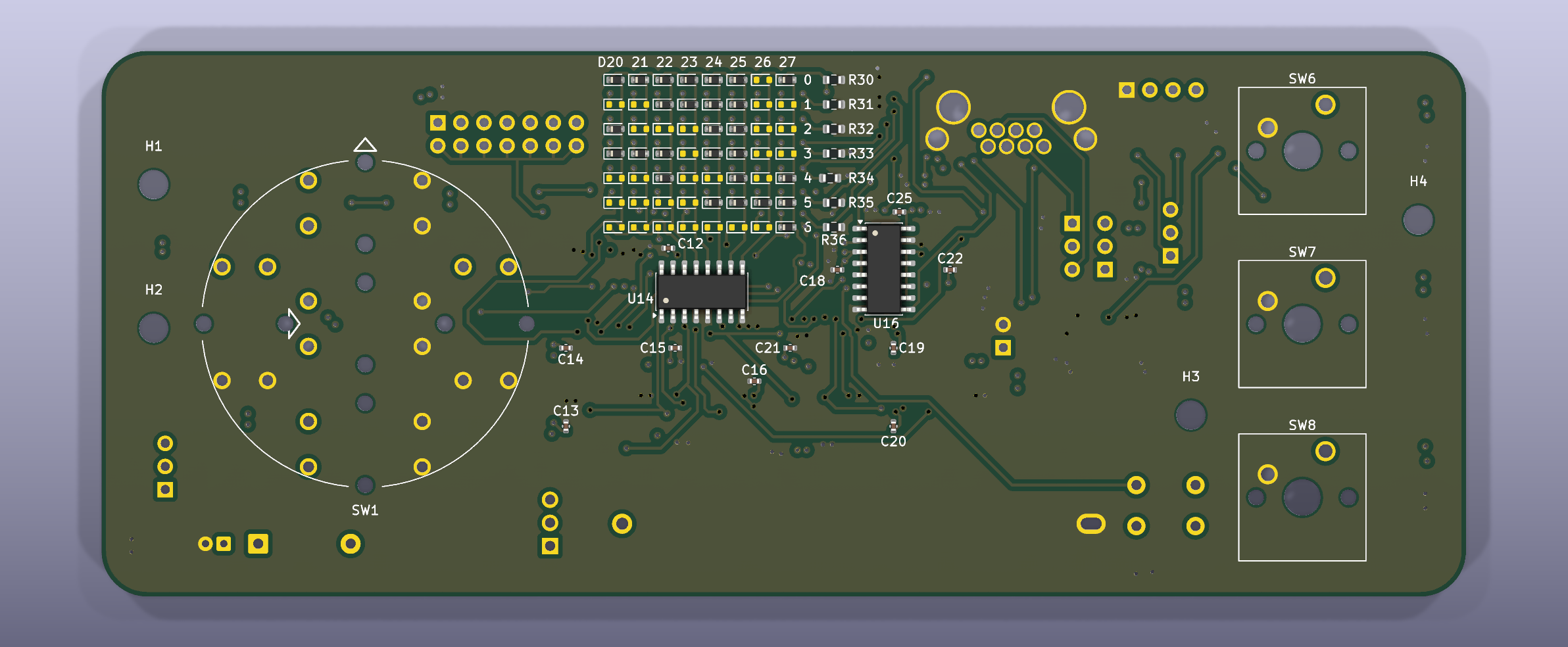
The silkscreen labels the grid like a table, since 56 designators would not
fit. Across the top is D20 21 22 … 27, one label per key column. Down the
right side is 0–6, one per bit, next to that bit's pull-down R30–R36. A
diode's designator is the label above it followed by the digit beside it.
0x80 | code and a release sends code. Bit 7
carries the key's state, which gives a game true key-down/key-up events.J3 (TTL header): 1 GND · 2 TXD out · 3 RXD (the far end's console, as 3.3 V TTL) · 4 +3.3 V, in or out depending on JP1.
For a PC instead, set JP4 to 2-3 and plug a 3.3 V USB-serial adapter into J3.
Three parts have requirements the footprint alone doesn't capture:
Before any copper was ordered, the design's netlist was run in a purpose-built logic simulator that models every IC against its datasheet truth table. Switches were driven through the real RC debounce values, and the serial output was decoded like a real UART receiver. The runs covered:
The simulator isn't part of this repository. The schematic passes KiCad ERC with no errors, and the board passes DRC and matches the schematic.
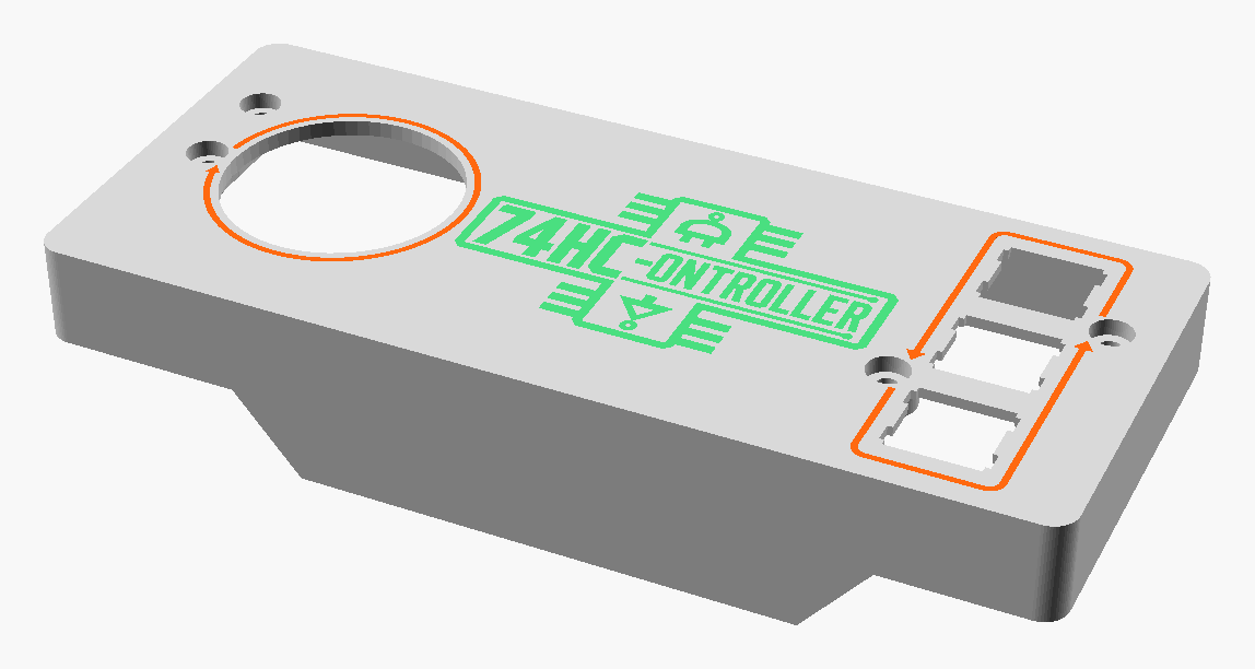
A three-piece 3D-printed enclosure, ready to slice, in case/:
| File | Part | |
|---|---|---|
top_with_trim.3mf | top shell, holding the switches | three colours: plate, trim and logo inlays. Print plate side down, no supports |
bottom.3mf | bottom shell | print on its raised hump. Support only the flat undersides (grid supports, build plate only, 2–3 interface layers, a brim) |
door.3mf | battery door | outer face down, no supports |
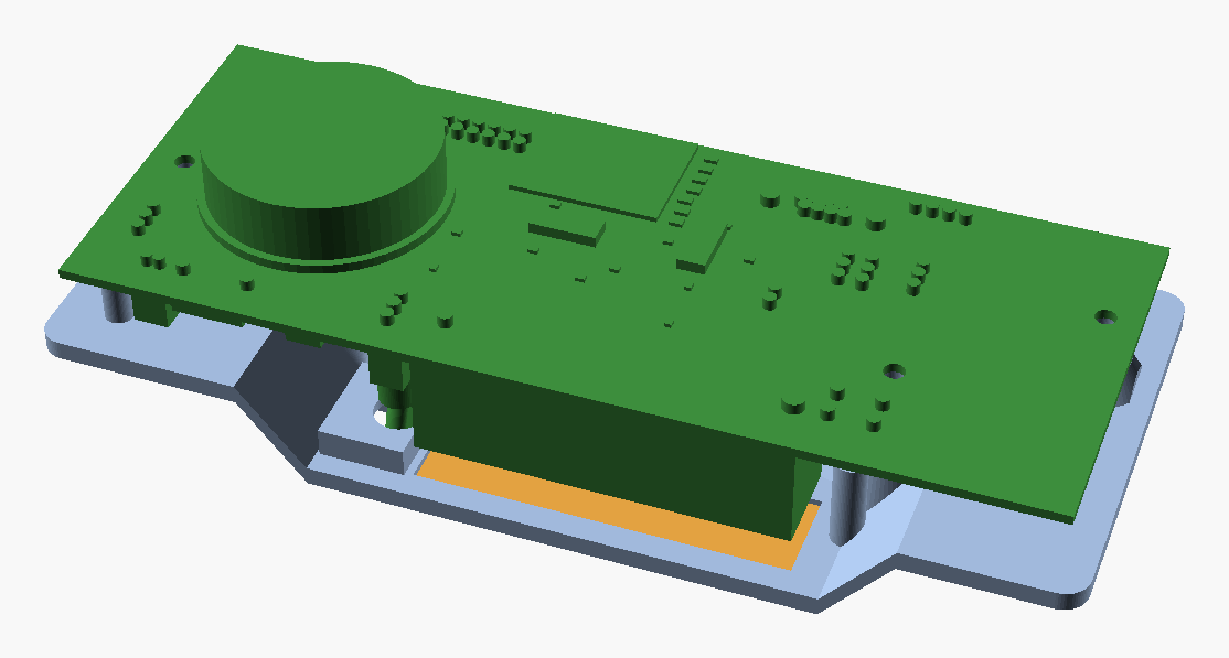
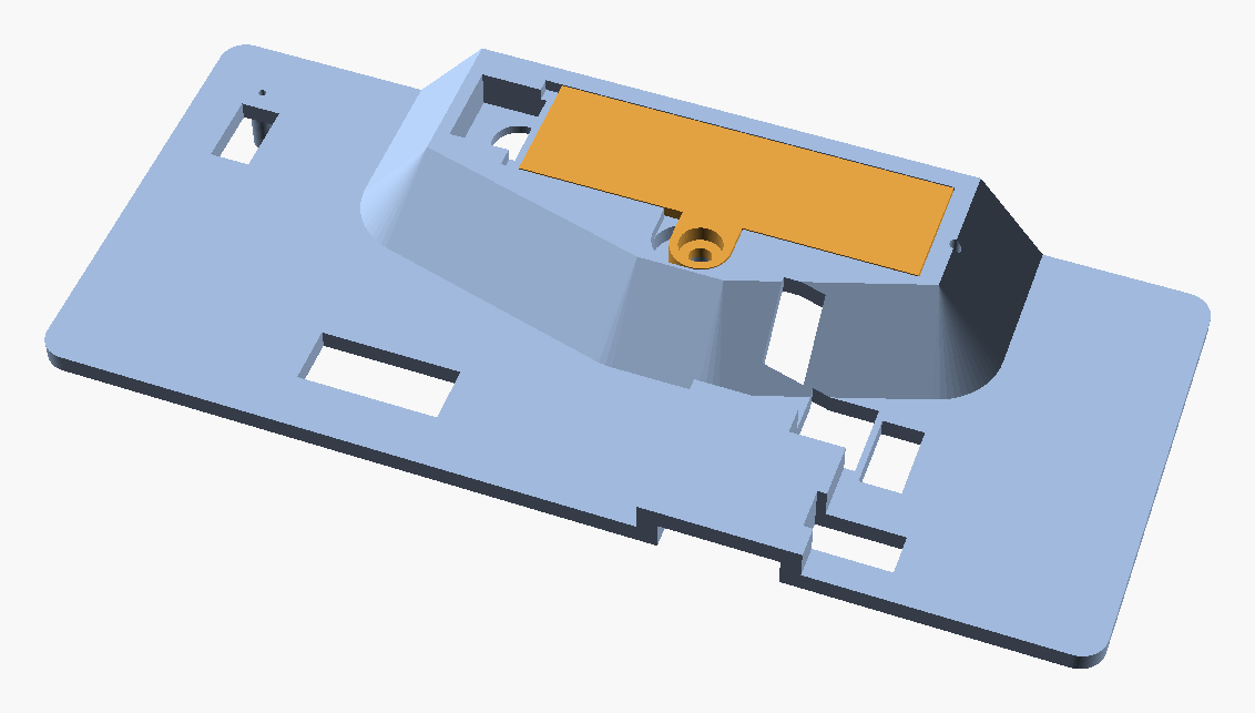
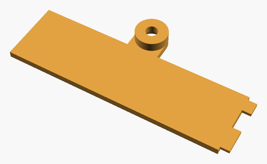
The case is shaped to be held in both hands from the ends. The bottom steps down only where the tall parts are (the battery, power switch and RJ45) and slopes up everywhere else. It has:
Hardware: five M3 × 8 pan-head screws and five M3 heat-set inserts, which go in 4.2 mm holes up to 8 mm deep.
Assembly:
kicad/logic-macropad.kicad_pro in KiCad 10 or newer
and plot gerbers and drill files. The project is self-contained, with its
own symbol and footprint libraries. Order 6 layers, 1.6 mm, FR-4. Nothing
on the board is impedance-sensitive, so any standard stackup works.kicad-cli sch export bom, lists them. The 29 unused ROM positions and
R53 are marked do not populate.kicad/ the KiCad 10 project
logic-macropad.kicad_pro project, design rules
logic-macropad.kicad_sch root sheet: block diagram, the seven stages
01_power_clock.kicad_sch stage 1 power, clock, reset
02_keys_debounce.kicad_sch stage 2 keys and debounce
03_scanner.kicad_sch stage 3 scanner and memory
04_sequencer.kicad_sch stage 4 transmit sequencer
05_ascii_rom.kicad_sch stage 5 ASCII diode ROM
06_uart_tx.kicad_sch stage 6 UART shift register
07_output.kicad_sch stage 7 output stage
logic-macropad.kicad_pcb the 6-layer board
lib/, logic-macropad.pretty/ project symbols and footprints
case/ print-ready 3MF files for the enclosure
docs/
schematic.pdf the full schematic
images/ renders used in this README| Qty | Value | Footprint | References |
|---|---|---|---|
| 57 | 1N4148 | Diode_SMD:D_SOD-523 | D2, D200, D201, D202, D203, D204, D205, D206, D210, D211, D212, D213, D214, D215, D216, D220 +41 |
| 22 | 100n | Capacitor_SMD:C_0402_1005Metric | C2, C10, C11, C12, C13, C14, C15, C16, C17, C18, C19, C20, C21, C22, C23, C24 +6 |
| 11 | 10k | Resistor_SMD:R_0603_1608Metric | R8, R10, R12, R14, R16, R18, R20, R22, R24, R50, R51 |
| 11 | 1k | Resistor_SMD:R_0603_1608Metric | R5, R11, R13, R15, R17, R19, R21, R23, R25, R52, R54 |
| 9 | 1u | Capacitor_SMD:C_0805_2012Metric | C5, C30, C31, C32, C33, C34, C35, C36, C37 |
| 7 | 15k | Resistor_SMD:R_0603_1608Metric | R30, R31, R32, R33, R34, R35, R36 |
| 4 | M3 | MountingHole_3.2mm_M3 | H1, H2, H3, H4 |
| 2 | 30p | Capacitor_SMD:C_0402_1005Metric | C3, C4 |
| 2 | 74HC14 | Package_SO:SOIC-14_3.9x8.7mm_P1.27mm | U2, U3 |
| 2 | 74HC151 | Package_SO:SOIC-16_3.9x9.9mm_P1.27mm | U5, U7 |
| 2 | 74HC161 | Package_SO:SOIC-16_3.9x9.9mm_P1.27mm | U4, U10 |
| 2 | 74HC165 | Package_SO:SOIC-16_3.9x9.9mm_P1.27mm | U15, U16 |
| 1 | 100R | Resistor_SMD:R_0603_1608Metric | R7 |
| 1 | 100k | Resistor_SMD:R_0603_1608Metric | R6 |
| 1 | 100u/16V | Capacitor_THT:CP_Radial_D5.0mm_P2.00mm | C1 |
| 1 | 10u | Capacitor_SMD:C_0805_2012Metric | C6 |
| 1 | 1M | Resistor_SMD:R_0603_1608Metric | R4 |
| 1 | 1N5817 | Diode_THT:D_DO-41_SOD81_P10.16mm_Horizontal | D3 |
| 1 | 1x AA | logic-macropad:BatteryHolder_MYOUNG_BH-AA-A1AJ020_1xAA | BT1 |
| 1 | 2k2 | Resistor_SMD:R_0603_1608Metric | R53 |
| 1 | 3.6864MHz | Crystal:Crystal_SMD_HC49-SD_HandSoldering | Y1 |
| 1 | 33u | Inductor_SMD:L_Cenker_CKCS5040 | L1 |
| 1 | 4k7 | Resistor_SMD:R_0603_1608Metric | R3 |
| 1 | 74HC08 | Package_SO:SOIC-14_3.9x8.7mm_P1.27mm | U12 |
| 1 | 74HC138 | Package_SO:SOIC-16_3.9x9.9mm_P1.27mm | U11 |
| 1 | 74HC238 | Package_SO:SOIC-16_3.9x9.9mm_P1.27mm | U14 |
| 1 | 74HC259 | Package_SO:SOIC-16_3.9x9.9mm_P1.27mm | U6 |
| 1 | 74HC32 | Package_SO:SOIC-14_3.9x8.7mm_P1.27mm | U13 |
| 1 | 74HC4060 | Package_SO:SOIC-16_3.9x9.9mm_P1.27mm | U1 |
| 1 | 74HC74 | Package_SO:SOIC-14_3.9x8.7mm_P1.27mm | U9 |
| 1 | 74HC86 | Package_SO:SOIC-14_3.9x8.7mm_P1.27mm | U8 |
| 1 | BAUD SEL | Connector_PinHeader_2.54mm:PinHeader_2x07_P2.54mm_Vertical | JP2 |
| 1 | BOTH | Jumper:SolderJumper-2_P1.3mm_Open_RoundedPad1.0x1.5mm | JP5 |
| 1 | BREAK EN | Connector_PinHeader_2.54mm:PinHeader_1x02_P2.54mm_Vertical | JP3 |
| 1 | CONSOLE | logic-macropad:RJ45_8P8C_Shielded_HCTL_HC-RJ45-5JA-1-4 | J2 |
| 1 | CTS | Jumper:SolderJumper-2_P1.3mm_Open_RoundedPad1.0x1.5mm | JP9 |
| 1 | DSR | Jumper:SolderJumper-2_P1.3mm_Open_RoundedPad1.0x1.5mm | JP8 |
| 1 | MAX3232 | Package_SO:SOIC-16_3.9x9.9mm_P1.27mm | U17 |
| 1 | ME2108A33 | Package_TO_SOT_SMD:SOT-23 | U18 |
| 1 | MX6 | Button_Switch_Keyboard:SW_Cherry_MX_1.00u_PCB | SW6 |
| 1 | MX7 | Button_Switch_Keyboard:SW_Cherry_MX_1.00u_PCB | SW7 |
| 1 | MX8 | Button_Switch_Keyboard:SW_Cherry_MX_1.00u_PCB | SW8 |
| 1 | NavPad5 | logic-macropad:SW_NavPad5_12x12_SJMS | SW1 |
| 1 | OUT MODE | Connector_PinHeader_2.54mm:PinHeader_1x03_P2.54mm_Vertical | JP4 |
| 1 | POWER | logic-macropad:SW_Toggle_SPDT_ST-0-102 | SW10 |
| 1 | PWR | LED_SMD:LED_0805_2012Metric_Pad1.15x1.40mm_HandSolder | D1 |
| 1 | PWR SEL | Connector_PinHeader_2.54mm:PinHeader_1x03_P2.54mm_Vertical | JP1 |
| 1 | RESET | Button_Switch_THT:SW_PUSH_6mm | SW9 |
| 1 | RX ROUTE | Connector_PinHeader_2.54mm:PinHeader_1x03_P2.54mm_Vertical | JP7 |
| 1 | TTL UART | Connector_PinHeader_2.54mm:PinHeader_1x04_P2.54mm_Vertical | J3 |
| 1 | TX ROUTE | Connector_PinHeader_2.54mm:PinHeader_1x03_P2.54mm_Vertical | JP6 |
It measures 150 × 60 mm and has 6 copper layers, 1.6 mm thick.
170 parts, built around the MAX3232CSE+, ME2108A33M3G, 74HC14D and 74HC151D. The full list of its parts is on this page, with links to each part's symbol and footprint where PCBKit's library has them.
From the Greentalinjo/74HController repository on GitHub, at the commit this page was made from: the board is kicad/logic-macropad.kicad_pcb and its schematic kicad/01_power_clock.kicad_sch. PCBKit opens the board in the browser, with nothing to install.
Its repository states no licence, so its author keeps all rights: ask Greentalinjo before reusing the design.
o7-machinehum/flipper-blackhat
Linux based WiFi pentesting device for the Flipper Zero.


NOAA-PMEL/ASVCO2
Open Source Repository for the Autonomous Surface Vehicle CO2 (ASVCO2) gen2 system


bornhack/badge2025
This badge focuses on LoRa and wireless communication in general, as there are also WiFi and Bluetooth Low Energy included in the ESP32-C3 module.


