2 layers215.9 × 50.8 mm
Honeywell HPAx00-ESPHome
flaviut/Honeywell-HPAx00-ESPHome
Demo of current firmware version, HPA200HEPAFilterV2.yaml
27 parts17

 caccia78/PlancH
Open source desk button panel for Home Assistant: ESP32-S3, ESPHome, OLED display, 10 buttons and RGB backlight. KiCad sources, Gerbers and a 3D-printable stand.
PlancH is an open-source printed circuit board by caccia78, from the caccia78/PlancH repository on GitHub. It is a 2-layer board of 120 × 52 mm with 45 parts on 32 nets, routed with 454 tracks and 110 vias.
It is built around the CL21B104KBCNNNC, SK6812MINI-E and SKC6812RV, with the CL31A476MPHNNNE among its other parts. Its parts include 14 capacitors, 13 diodes, 10 switches, 2 ICs and 1 resistor. It belongs with the home automation and IoT and lEDs and displays boards and the ESP32 boards of this library.


A desk button panel for Home Assistant. Ten tactile buttons, a small OLED display, a touch area and thirteen addressable RGB LEDs on a black PCB that sits on your desk, either on its own rubber feet or on a 3D-printed stand. Powered by a Waveshare ESP32-S3-Zero running ESPHome, with native Home Assistant integration.
📖 Documentation: caccia78.github.io/PlancH
https://github.com/user-attachments/assets/e7710835-a2c8-45fb-a4f4-b32c819555f0
The video is also in media/ (MP4 and WebM).
Status: Rev. 1, prototypes on order. The design is complete and passes ERC/DRC, but the first boards have not been assembled and tested yet. Build one if you like to tinker, and expect changes.
| Front | Back |
|---|---|
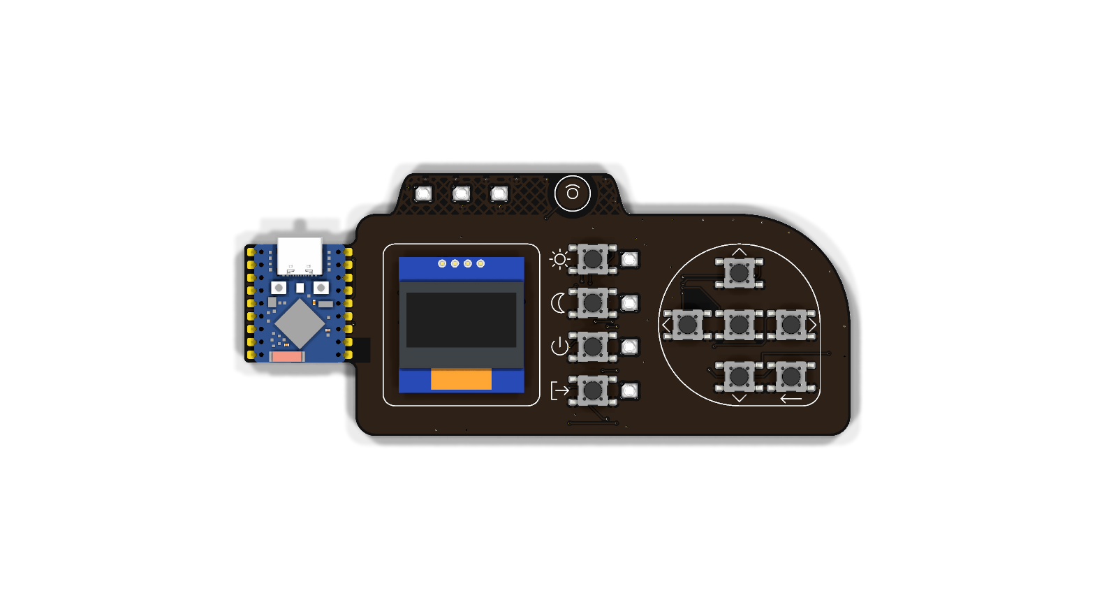 | 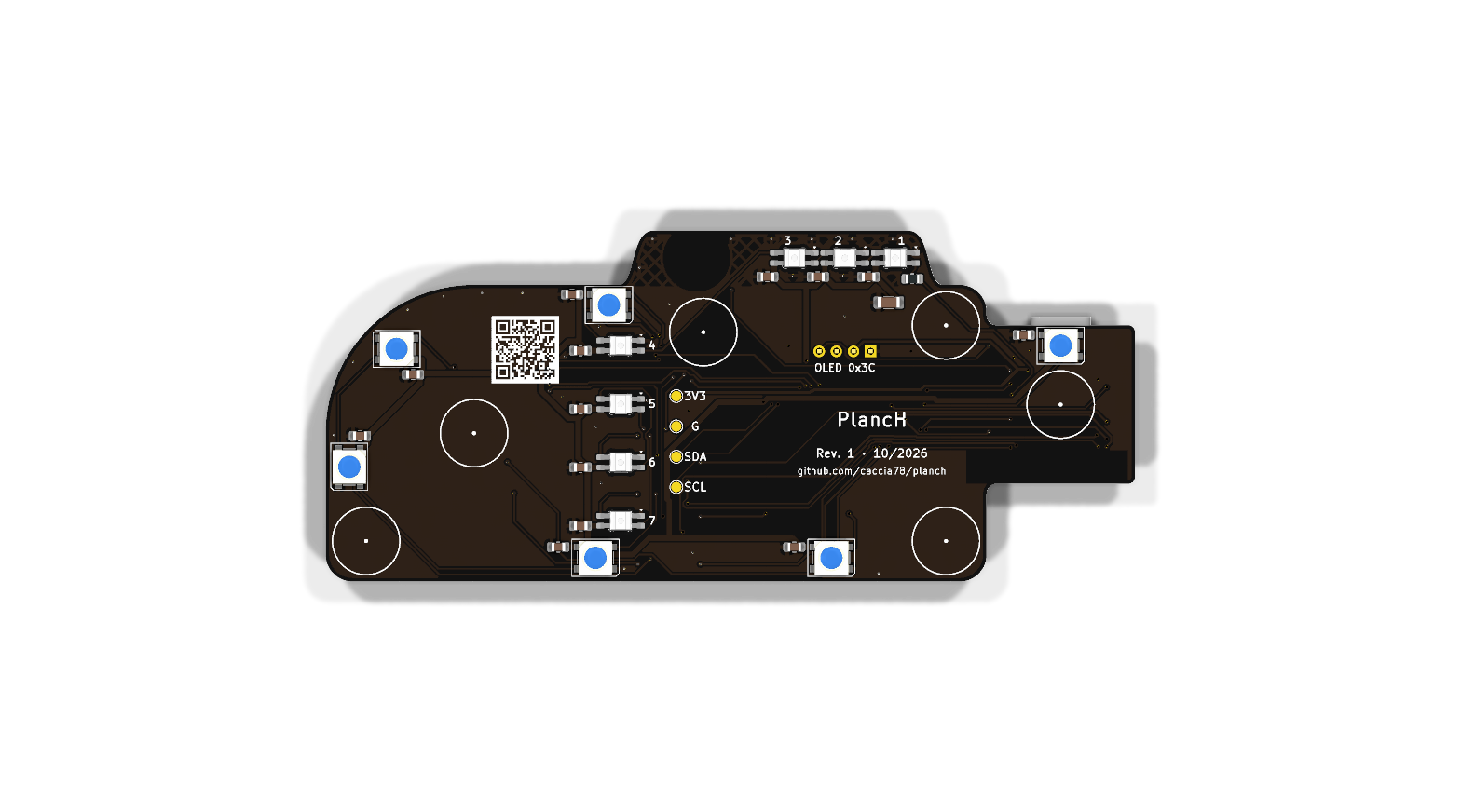 |
production/gerber/ (or the Gerber ZIP attached to the
latest release) to JLCPCB, PCBWay or any other maker.
Reference settings: 2 layers, 2.0 mm FR4 (1.6 mm works too), matte black solder mask,
white silkscreen, ENIG finish.production/planch-bom.csv, with manufacturer part numbers.production/planch-ibom.html in a browser:
the interactive BOM highlights every part on the board. Suggested order: passives and LEDs
on the back, buttons, ESP32 module, OLED last.esphome run firmware/planch.yaml and set the Wi-Fi after
flashing. Then install the Home Assistant package homeassistant/planch.yaml and put the
label PlancH on the devices to control: the panel finds them by itself, by room.The project website has the full documentation: components with shop links, PCB ordering, a step-by-step assembly guide, firmware and Home Assistant setup.
hardware/      KiCad 10 project: schematic, PCB, custom symbols, footprints and 3D models
production/    Gerber and drill files, BOM, pick-and-place, interactive BOM, schematic PDF, STEP
mechanical/    3D-printable accessories (build123d sources, STL, 3MF, STEP)
firmware/      ESPHome: planch.yaml (board), planch-bringup.yaml (assembly test), planch-test.yaml (test bench)
homeassistant/ Home Assistant package (menu from labels and areas) and test bench dashboard
media/ renders and videoPlancH is open source hardware.
See LICENSE.md for details. The source location printed on the back of the board
is github.com/caccia78/planch.
© 2026 Vincenzo Cacciatore
| Qty | Value | Footprint | References |
|---|---|---|---|
| 13 | 100n | Capacitor_SMD:C_0805_2012Metric_Pad1.18x1.45mm_HandSolder | C1, C2, C3, C4, C5, C6, C7, C8, C9, C10, C11, C12, C13 |
| 10 | PTS645SH43 | planch:SW_SPST_PTS645Sx43SMTR92_NoSilk | SW1, SW2, SW3, SW4, SW5, SW6, SW7, SW8, SW9, SW10 |
| 7 | SK6812MINI-E | planch:LED_SK6812MINI-E_3.2x2.8mm_P1.5mm_ReverseMount_HandSolder | D1, D2, D3, D4, D5, D6, D7 |
| 6 | SK6812 5050 RGB | LED_SMD:LED_SK6812_PLCC4_5.0x5.0mm_P3.2mm | D8, D9, D10, D11, D12, D13 |
| 1 | 330 | Resistor_SMD:R_0805_2012Metric_Pad1.20x1.40mm_HandSolder | R1 |
| 1 | 3V3 | TestPoint:TestPoint_Pad_D1.5mm | TP1 |
| 1 | 47u | Capacitor_SMD:C_1206_3216Metric_Pad1.33x1.80mm_HandSolder | C14 |
| 1 | ESP32-S3-Zero | planch:Waveshare_ESP32-S3-Zero_Castellated | U1 |
| 1 | GND | TestPoint:TestPoint_Pad_D1.5mm | TP2 |
| 1 | OLED 0.96in SSD1306 | planch:OLED_SSD1306_0.96in_I2C_24.8x26.9mm | U2 |
| 1 | SCL | TestPoint:TestPoint_Pad_D1.5mm | TP4 |
| 1 | SDA | TestPoint:TestPoint_Pad_D1.5mm | TP3 |
| 1 | Touch | planch:TouchPad_D6mm_Covered | E1 |
It measures 120 × 52 mm and has 2 copper layers, 2 mm thick.
45 parts, built around the CL21B104KBCNNNC, SK6812MINI-E, SKC6812RV and CL31A476MPHNNNE. The full list of its parts is on this page, with links to each part's symbol and footprint where PCBKit's library has them.
From the caccia78/PlancH repository on GitHub, at the commit this page was made from: the board is hardware/planch/planch.kicad_pcb and its schematic hardware/planch/planch.kicad_sch. PCBKit opens the board in the browser, with nothing to install.
Its repository states no licence, so its author keeps all rights: ask caccia78 before reusing the design.
flaviut/Honeywell-HPAx00-ESPHome
Demo of current firmware version, HPA200HEPAFilterV2.yaml

MartinDrillon/CLAVICORE
Pilotage d’un clavecin à distance grâce à un clavier ergonomique.


stefanskotte/Nano-Tek
A tiny, modern reimagining of the classic Gotek floppy-disk-drive emulator. Nano-Tek keeps the full feature set of a Gotek-style FDD emulator but packs it onto a board that is a fraction of the size, hence the name…


