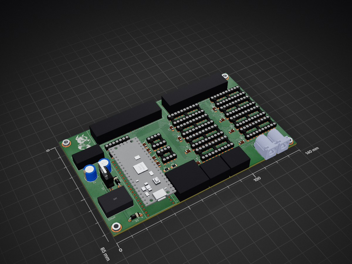
4 layers140 × 85 mm
Hub Router PCB
bu-gsLab/Hardware
Repository of hardware designs for Detector Lab work. All designs when possible should be done using Autodesk Inventor 2019 or earlier.
14 parts1
 bu-gsLab/Hardware1
Repository of hardware designs for Detector Lab work. All designs when possible should be done using Autodesk Inventor 2019 or earlier.
Gantry Hub V2 PCB is an open-source printed circuit board by bu-gsLab, from the bu-gsLab/Hardware repository on GitHub. It is a 4-layer board of 140 × 85 mm with 47 parts on 167 nets, routed with 917 tracks and 25 vias.
It is built around the SC0915, SN74AHCT125N and LM2575-5.0WT, with the LM358, MCP4802-E/P and TPIC6B595N among its other parts. Its parts include 14 capacitors, 13 ICs, 8 connectors, 4 resistors and 2 diodes.


Repository of hardware designs for Detector Lab work. All designs when possible should be done using Autodesk Inventor 2019 or earlier.
Any shop jobs, based on these designs or otherwise, must have an accompanying work order in Work Orders/. Start with the appropriate blank form (found in Work Orders/), then include your and your supervisor's contact into, the date, and a short description of the job. Export the form as a PDF and upload it to the repository. Next, create an Issue in this repository with a more detailed description of the job. Add any relevant tags to the issue and assign it to the correct project. When the job is finished, resolve the issue.
Work order forms should follow the following naming convention: YYYY_MM_{PROJECT}_{DESC}.pdf
| Qty | Value | Footprint | References |
|---|---|---|---|
| 10 | 0.1uF | Capacitor_SMD:C_1206_3216Metric_Pad1.33x1.80mm_HandSolder | C3, C4, C6, C8, C9, C10, C11, C12, C13, C14 |
| 8 | TPIC6B595N | Package_DIP:DIP-20_W7.62mm_Socket_LongPads | U1, U4, U8, U9, U10, U11, U12, U13 |
| 4 | MountingHole_Pad | MountingHole:MountingHole_3.2mm_M3_Pad_Via | H1, H2, H3, H5 |
| 2 | 10k | Resistor_SMD:R_1206_3216Metric_Pad1.30x1.75mm_HandSolder | R2, R3 |
| 2 | 10uF | Capacitor_SMD:C_1206_3216Metric_Pad1.33x1.80mm_HandSolder | C5, C7 |
| 2 | 14.3k | Resistor_SMD:R_1206_3216Metric_Pad1.30x1.75mm_HandSolder | R4, R5 |
| 2 | 178-025-513R571 | lib_footprints:CONN_178-025-513_NRC | J2, J6 |
| 2 | Barrel_Jack | lib_footprints:CUI PJ-037A | J7, J8 |
| 2 | Mini-DIN-4 | lib_footprints:CUI_MD-40SM | J4, J5 |
| 1 | 100uF | Capacitor_THT:CP_Radial_D8.0mm_P3.50mm | C1 |
| 1 | 11DQ06 | Diode_THT:D_DO-41_SOD81_P7.62mm_Horizontal | D1 |
| 1 | 11DQ06 | Diode_THT:D_A-405_P7.62mm_Horizontal | D2 |
| 1 | 330uF | Capacitor_THT:CP_Radial_D8.0mm_P3.50mm | C2 |
| 1 | 330uH | lib_footprints:IND_PE-526xx_V_PUL | L1 |
| 1 | Conn_01x02_Socket | lib_footprints:CONN_SDA_43255-00xx_02_MOL | J1 |
| 1 | DIN-8 | lib_footprints:CUI_SDF-80J | J3 |
| 1 | LM2575-5.0WT | Package_TO_SOT_THT:TO-220-5_Vertical | U3 |
| 1 | LM358 | Package_DIP:DIP-8_W7.62mm_Socket_LongPads | U5 |
| 1 | LOGO | lib_footprints:Rhett | G*** |
| 1 | MCP4802 | Package_DIP:DIP-8_W7.62mm_Socket_LongPads | U6 |
| 1 | SC0915 | lib_footprints:SC0915 | U2 |
| 1 | SN74AHCT125N | Package_DIP:DIP-14_W7.62mm_Socket_LongPads | U7 |
bu-gsLab/Hardware
Repository of hardware designs for Detector Lab work. All designs when possible should be done using Autodesk Inventor 2019 or earlier.


fedecastellaro/AD7124-4-Implementation
AD7124-4 - 24-Bit ADC, 4-Channel , Sigma-Delta - PCB and software implementation


It measures 140 × 85 mm and has 4 copper layers, 1.6 mm thick.
47 parts, built around the SC0915, SN74AHCT125N, LM2575-5.0WT and LM358. The full list of its parts is on this page, with links to each part's symbol and footprint where PCBKit's library has them.
From the bu-gsLab/Hardware repository on GitHub, at the commit this page was made from: the board is General Gantry/Gantry Hub V2/Gantry Hub V2 PCB/Gantry Hub V2 PCB.kicad_pcb and its schematic General Gantry/Gantry Hub V1/Hub Router PCB/Hub Router PCB.kicad_sch. PCBKit opens the board in the browser, with nothing to install.
Its repository states no licence, so its author keeps all rights: ask bu-gsLab before reusing the design.