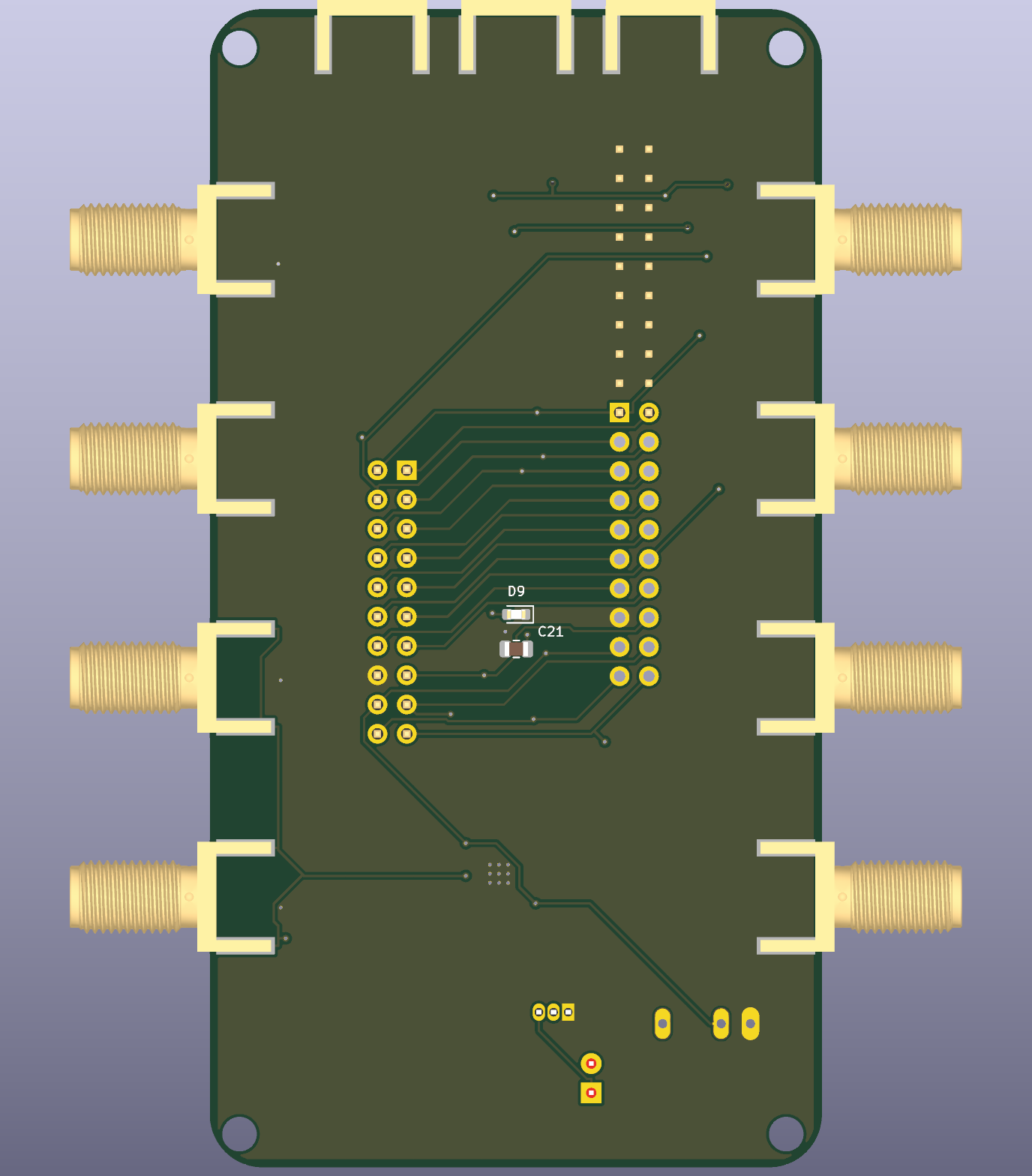
2 layers53.1 × 100.5 mm

 aryakaithal8/Jammer
A jamming device which jam everything
Jammer is an open-source printed circuit board by aryakaithal8, from the aryakaithal8/Jammer repository on GitHub. It is a 2-layer board of 53.1 × 100.5 mm with 94 parts on 118 nets, routed with 2,167 tracks and 204 vias.
It is built around the ESP32-S3-WROOM-1-N8, PCF8574T and IP5306, with the WS2812B-2020, S8050 and AO3401A among its other parts. Its parts include 35 resistors, 19 capacitors, 10 switches, 7 diodes and 6 ICs. It belongs with the ESP32 boards of this library.


Jammer is my custom handheld electronics project, built around an ESP32-S3-WROOM-1-N16 with a main board, a separate shield and a custom enclosure.
so basically i wanted to make a handheld device with its own screen, buttons, battery and a proper case, but i also wanted to go further than just connecting a bunch of ready-made modules together.. custom schematics, a stacked PCB design, touch display, storage, infrared, status feedback and the firmware side too. i designed the electronics in KiCad and worked on the enclosure in Fusion 360, which turned into a much bigger rabbit hole than expected lol
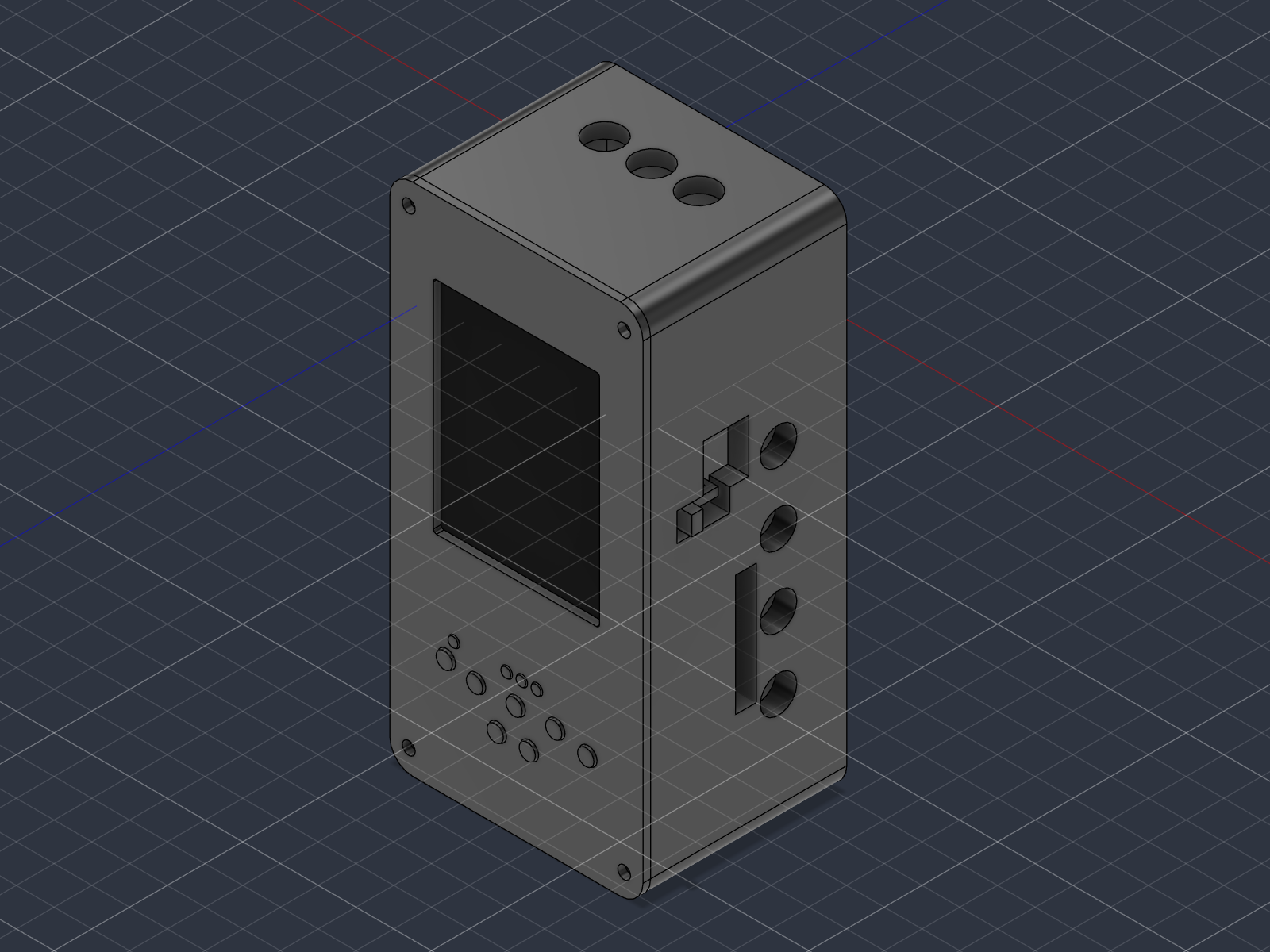
i wanted to build something where i could work on the whole thing from scratch instead of only doing one small part of it.. the circuit, board layout, case, controls and the parts list all had to fit together into one handheld project
main goals :
the fun part is that everything affects everything else.. changing a connector position can affect the routing and the case opening, while changing the display arrangement can affect the buttons, internal space and cable clearance. thats the kind of detail that makes a handheld project way more involved than it looks from the outside
whats in this repo :
CAD/ — exported assembly models and printing filesBOM Images/ — supplier and component sourcing screenshotsFirmware/ — MicroPython application files and the bundled runtime imageFusionFiles/ — editable Fusion 360 design fileImages/ — PCB, schematic and enclosure screenshotsPCB/ — KiCad projects, libraries, audit material and the separate engineering revisionPDFs/ — exported schematic and layout PDFsProduction/ — Gerber archives, placement information, BOM and netlist exportsbom.csv — sourcing list, supplier links and captured costs| Project | Jammer |
| Format | Custom handheld device with stacked main and shield boards |
| Controller listed in BOM | ESP32-S3-WROOM-1-N16 |
| Display | Robu 62026 2.8-inch SPI touch display |
| Front controls | Six buttons shown in the project design |
| USB | Two USB-C receptacles listed in the BOM |
| Development interface | CP2102N USB-to-UART section |
| Button interface in earlier design | PCF8574 I/O expander |
| Storage | SD card socket included in the design |
| Infrared | IR emitter and receiver parts included in the project |
| Feedback | Status LEDs, addressable RGB and a buzzer section |
| Radio parts in the supplied design material | nRF24L01-family and CC1101 parts with external connector provisions |
| Power | Battery, charging and supply sections with revision-specific parts |
| PCB | Main board and shield, with four-layer fabrication files in the revised engineering package |
| CAD | Fusion 360 and exported 3D files |
| Firmware | MicroPython source with hardware limitations documented in the files |
some of the interesting work is hidden inside the enclosure.. the boards need to fit together, the display needs its own space and support, and the controls and connectors need to line up with the outside of the case. the CAD and PCB images below show the project from a few different angles
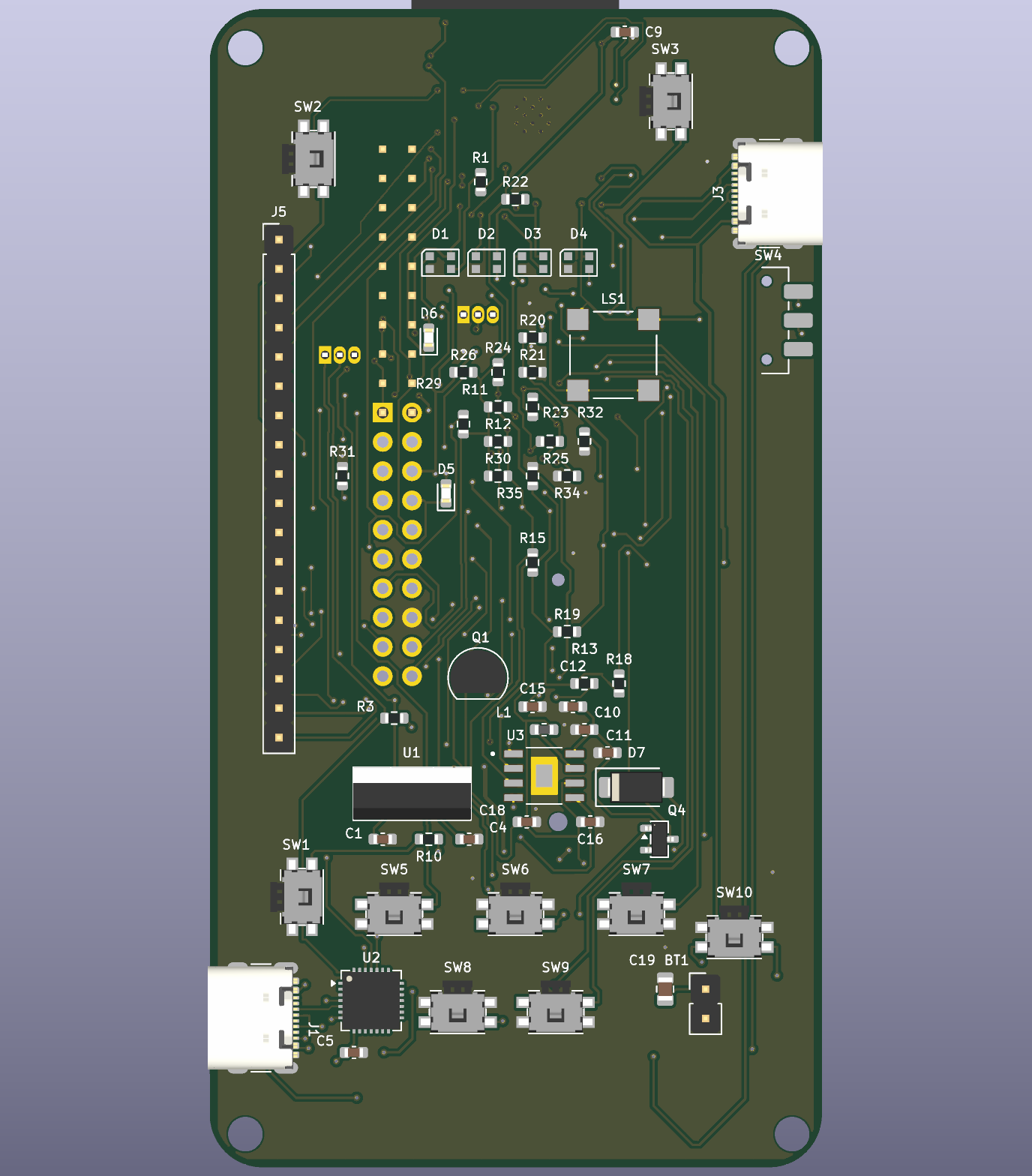
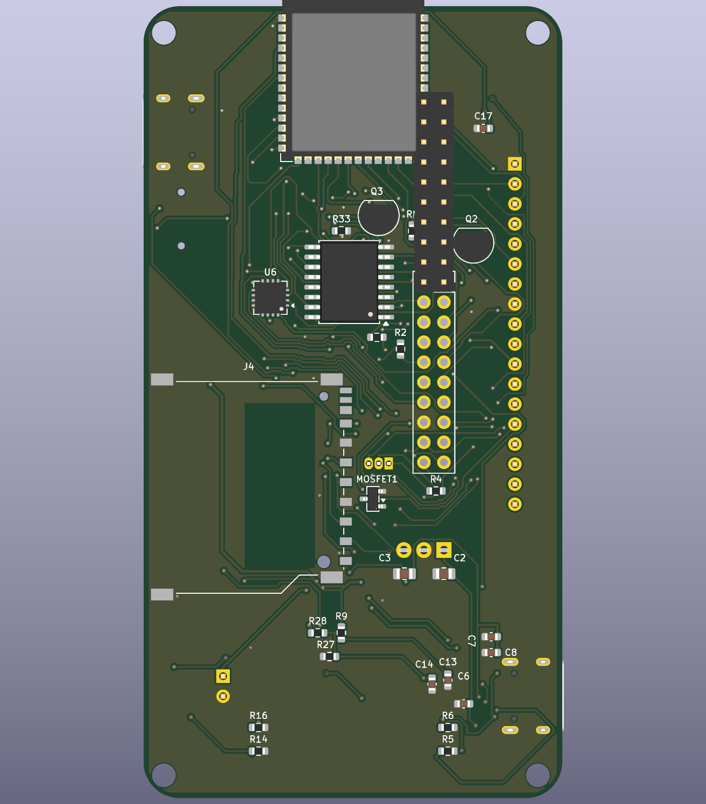
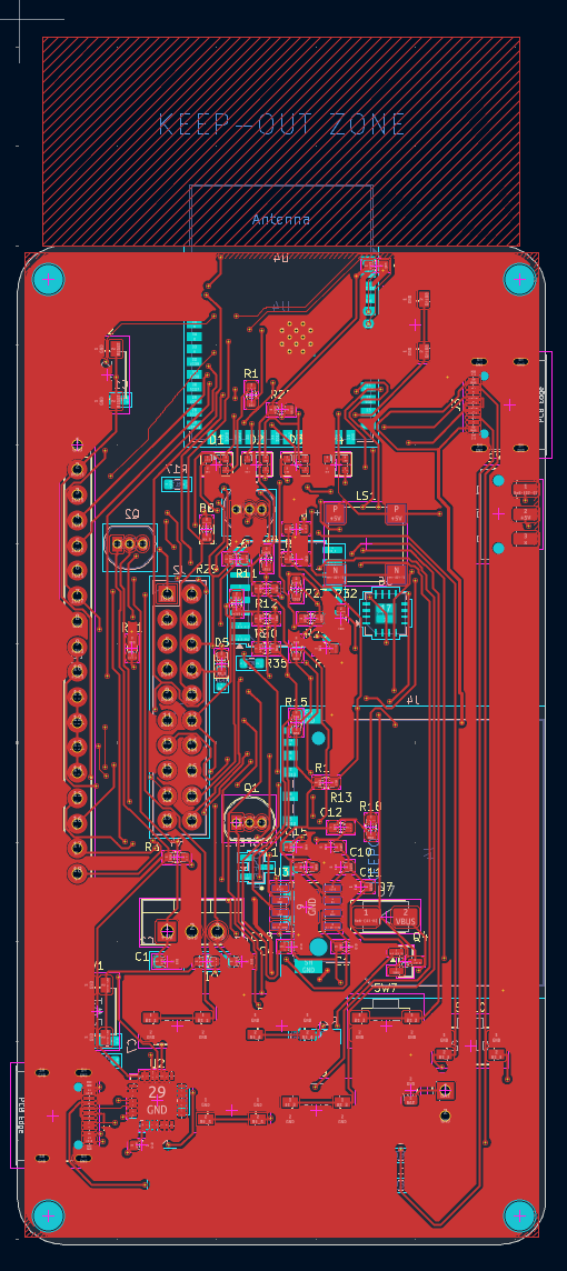
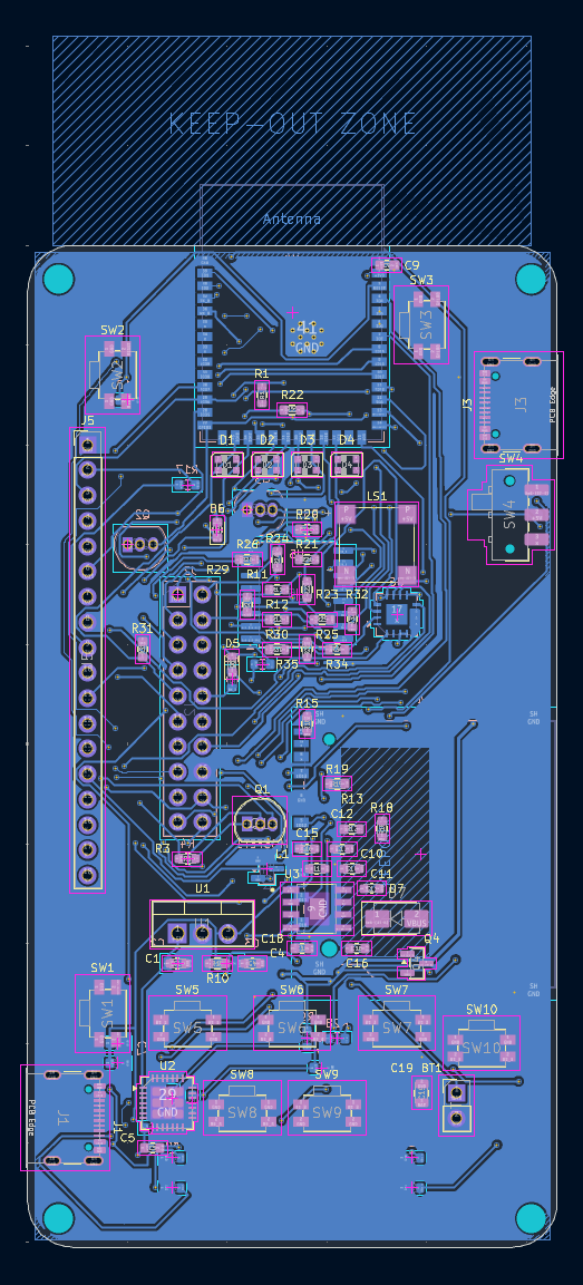
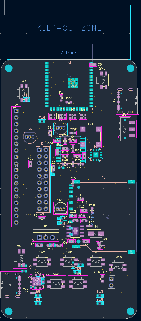
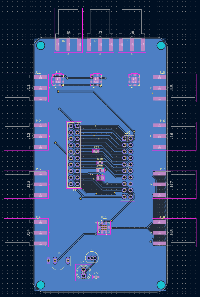
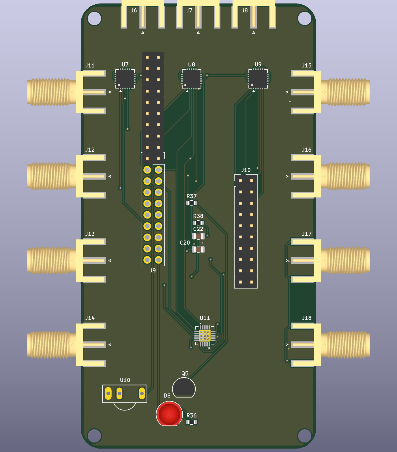
i worked on the schematic in smaller sections first, then brought those sections together before moving into the PCB layout. the screenshots include the controller, power, connectors, display, controls and supporting circuits from the supplied design material
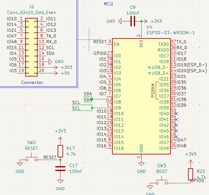
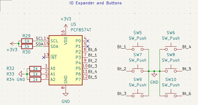
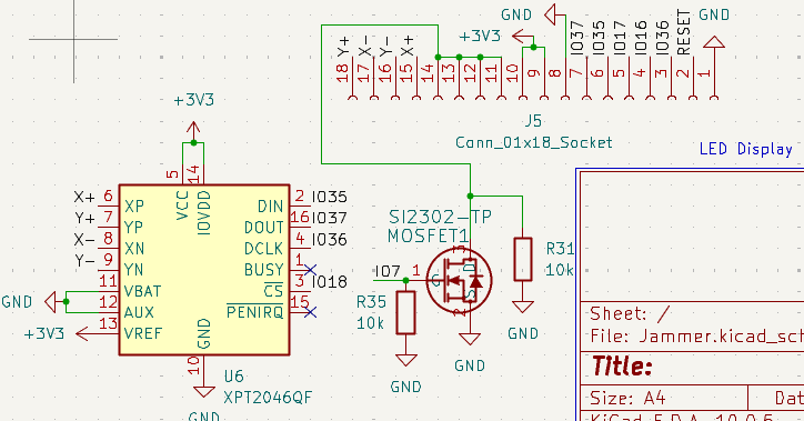
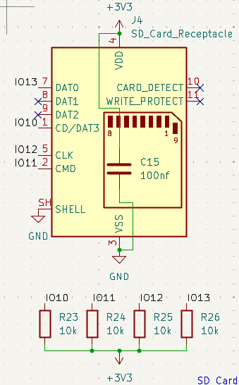
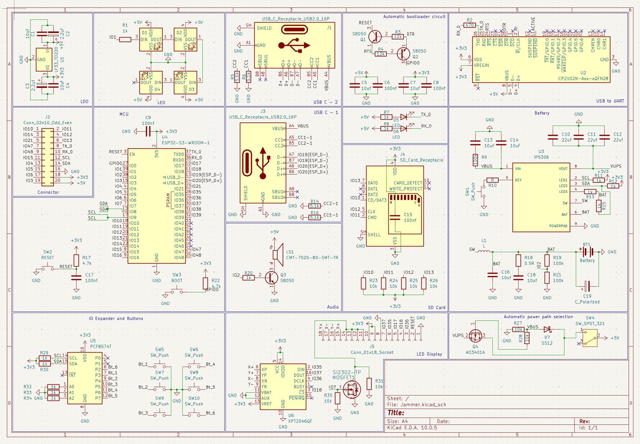
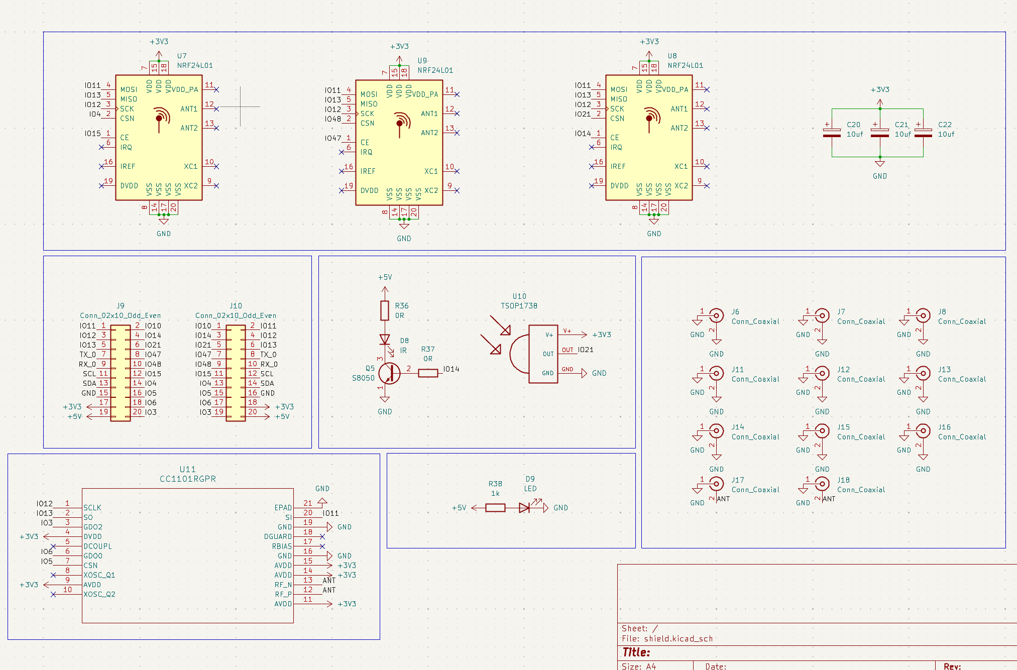
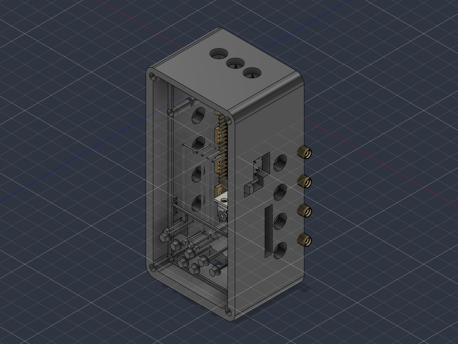
these are design screenshots and renders, so they show the intended arrangement rather than a finished physical assembly. some schematic images also show earlier revisions and should be read alongside the current files
the main project folder names are:
PCB/ — KiCad design files and engineering referencesCAD/ — assembly exports and printing filesFusionFiles/ — editable Fusion designFirmware/ — MicroPython source and runtime filesProduction/ — manufacturing outputsPDFs/ — schematic and layout exportsImages/ — project screenshots used in this READMEBOM Images/ — sourcing screenshotsbom.csv — captured sourcing listthe exact filenames inside each folder may change as the project gets updated, so open the folders to find the relevant versions. check the revision before combining a schematic, board, firmware file or parts list from different places
the case was designed in Fusion 360. FusionFiles/Jammer V1.f3d is the editable design, while CAD/ contains the exported assembly and printing material. check the available files and formats before preparing a print or manufacturing order
the case and PCB need to be checked together before fabrication: board mounting, screen support, connector access, button alignment and space for the battery and cables all matter. something looking clear in the outside render doesnt automatically mean the internal assembly fits properly
the internal CAD view is useful for seeing how the parts are intended to sit together, but the actual display module, connector tolerances and battery clearance still need a physical fit check
the project includes a Firmware/ folder with MicroPython files for the application, hardware interfaces, display, storage, infrared and radio-related code. it also includes an ESP32-S3 MicroPython runtime image and its provenance information
the application source includes menu and device-status handling, touch calibration, storage/logging support and interface-related functions. these are source-level features and still need to be checked on the actual hardware
the top-level hardware.py explicitly sets RADIOS_AVAILABLE = False. it also holds some conflicting functions inactive instead of pretending they are usable, so the presence of a menu item or driver file isnt proof that the matching hardware feature is ready
firmware configuration and flashing details should be confirmed against the actual files and the matching schematic revision before building. i dont want to claim a particular image, pin assignment or feature is ready until it has been checked against the board it is meant to run on
the sourcing bill of materials is in bom.csv. it includes the item name, quantity, supplier link, distributor and total line cost in US dollars.
listed BOM total: $459.58 USD
a few notable parts from the BOM:
| Part | Purpose |
|---|---|
| ESP32-S3-WROOM-1-N16 | Main controller |
| Robu 62026 touch display | Screen and touch interface |
| CP2102N-A02-GQFN28R | USB-to-UART interface |
| PCF8574T | I/O expansion in the earlier design |
| TE Connectivity 2041021-3 | SD card socket |
| GCT USB4105-GF-A | USB-C receptacles |
| WS2812B-2020-V6 | Addressable RGB indicators |
| CMT-7525-80-SMT-TR | Buzzer listed in the sourcing list |
| TSAL6200 and TSOP1738 | Infrared-related parts |
| nRF24L01 and CC1101 parts | Radio hardware represented in the supplied design material |
| Main and shield PCB fabrication | Separate board orders listed in the CSV |
| Printed enclosure and mounting hardware | Case and assembly parts |
| Qty | Value | Footprint | References |
|---|---|---|---|
| 13 | 1k | Resistor_SMD:R_0603_1608Metric | R1, R7, R8, R11, R12, R13, R15, R20, R29, R30, R32, R33, R34 |
| 8 | 10k | Resistor_SMD:R_0603_1608Metric | R23, R24, R25, R26, R27, R28, R31, R35 |
| 8 | 10uf | Capacitor_SMD:C_0603_1608Metric | C1, C4, C5, C7, C13, C14, C16, C18 |
| 7 | SW_Push | Button_Switch_SMD:Panasonic_EVQPUJ_EVQPUA | SW1, SW5, SW6, SW7, SW8, SW9, SW10 |
| 5 | 100nf | Capacitor_SMD:C_0603_1608Metric | C6, C8, C9, C15, C17 |
| 4 | 5.1k | Resistor_SMD:R_0603_1608Metric | R5, R6, R14, R16 |
| 4 | M2.5 / 3 mm NPTH | MountingHole_3mm_M2p5 | H1, H2, H3, H4 |
| 4 | WS2812B-2020 | LED_SMD:LED_WS2812B-2020_PLCC4_2.0x2.0mm | D1, D2, D3, D4 |
| 3 | 100k | Resistor_SMD:R_0603_1608Metric | R9, R19, R21 |
| 3 | 22uf | Capacitor_SMD:C_0603_1608Metric | C10, C11, C12 |
| 3 | S8050 | Package_TO_SOT_THT:TO-92_Inline | Q1, Q2, Q3 |
| 2 | 12k | Resistor_SMD:R_0603_1608Metric | R3, R4 |
| 2 | 2.2uf | Capacitor_SMD:C_0805_2012Metric | C2, C3 |
| 2 | 4.7k | Resistor_SMD:R_0603_1608Metric | R17, R22 |
| 2 | LED | LED_SMD:LED_0603_1608Metric | D5, D6 |
| 2 | USB_C_Receptacle_USB2.0_16P | Connector_USB:USB_C_Receptacle_GCT_USB4105-xx-A_16P_TopMnt_Horizontal | J1, J3 |
| 1 | 0.5R | Resistor_SMD:R_0603_1608Metric | R18 |
| 1 | 470 | Resistor_SMD:R_0603_1608Metric | R2 |
| 1 | AO3401A | Package_TO_SOT_SMD:SOT-23 | Q4 |
| 1 | BOOT | Button_Switch_SMD:Panasonic_EVQPUJ_EVQPUA | SW3 |
| 1 | Battery | Connector_PinHeader_2.54mm:PinHeader_1x02_P2.54mm_Vertical | BT1 |
| 1 | CMT-7525-80-SMT-TR | CMT-7525-80-SMT-TR:XDCR_CMT-7525-80-SMT-TR | LS1 |
| 1 | CP2102N-Axx-xQFN28 | Package_DFN_QFN:QFN-28-1EP_5x5mm_P0.5mm_EP3.35x3.35mm | U2 |
| 1 | C_Polarized | Capacitor_SMD:C_0805_2012Metric | C19 |
| 1 | Conn_01x18_Socket | Connector_PinHeader_2.54mm:PinHeader_1x18_P2.54mm_Vertical | J5 |
| 1 | Conn_02x10_Odd_Even | Connector_PinHeader_2.54mm:PinHeader_2x10_P2.54mm_Vertical | J2 |
| 1 | ESP32-S3-WROOM-1 | RF_Module:ESP32-S3-WROOM-1 | U4 |
| 1 | IP5306 | IP5306:SOP127P600X165-9N | U3 |
| 1 | L | Inductor_SMD:L_0603_1608Metric | L1 |
| 1 | LF33_TO220 | Package_TO_SOT_THT:TO-220-3_Vertical | U1 |
| 1 | PCF8574T | Package_SO:SOIC-16W_7.5x10.3mm_P1.27mm | U5 |
| 1 | R | Resistor_SMD:R_0603_1608Metric | R10 |
| 1 | RESET | Button_Switch_SMD:Panasonic_EVQPUJ_EVQPUA | SW2 |
| 1 | SD_Card_Receptacle | Connector_Card:SD_TE_2041021 | J4 |
| 1 | SI2302-TP | Package_TO_SOT_SMD:SOT-23 | MOSFET1 |
| 1 | SS12 | Diode_SMD:D_SMA | D7 |
| 1 | SW_SPDT_321 | Button_Switch_SMD:SW_SPDT_CK_JS102011SAQN | SW4 |
| 1 | XPT2046QF | Package_DFN_QFN:QFN-16-1EP_4x4mm_P0.65mm_EP2.1x2.1mm | U6 |


nyuad-space/dumpling
Modular payload for high-speed logging and benchmarking of COTS sensors, enabling real-world performance data and open sharing.

maximus64/opendiag-hardware
OpenDIAG - Open Source OBD2 Interface (Hardware)

RamRamAndroid/ESP32Drone-CodeMatrix
ESP32 Drone by CodeMatrix is a compact, WiFi-controlled drone based on the ESP32-S3 microcontroller. Designed for hobbyists, makers, and engineers, ESP32 Drone by CodeMatrix offers a simple yet powerful platform for…
It measures 53.1 × 100.5 mm and has 2 copper layers, 1.6 mm thick.
94 parts, built around the ESP32-S3-WROOM-1-N8, PCF8574T, IP5306 and WS2812B-2020. The full list of its parts is on this page, with links to each part's symbol and footprint where PCBKit's library has them.
From the aryakaithal8/Jammer repository on GitHub, at the commit this page was made from: the board is PCB/Jammer.kicad_pcb and its schematic PCB/Jammer.kicad_sch. PCBKit opens the board in the browser, with nothing to install.
Its repository states no licence, so its author keeps all rights: ask aryakaithal8 before reusing the design.