Skip to the content
PCBKitNew board
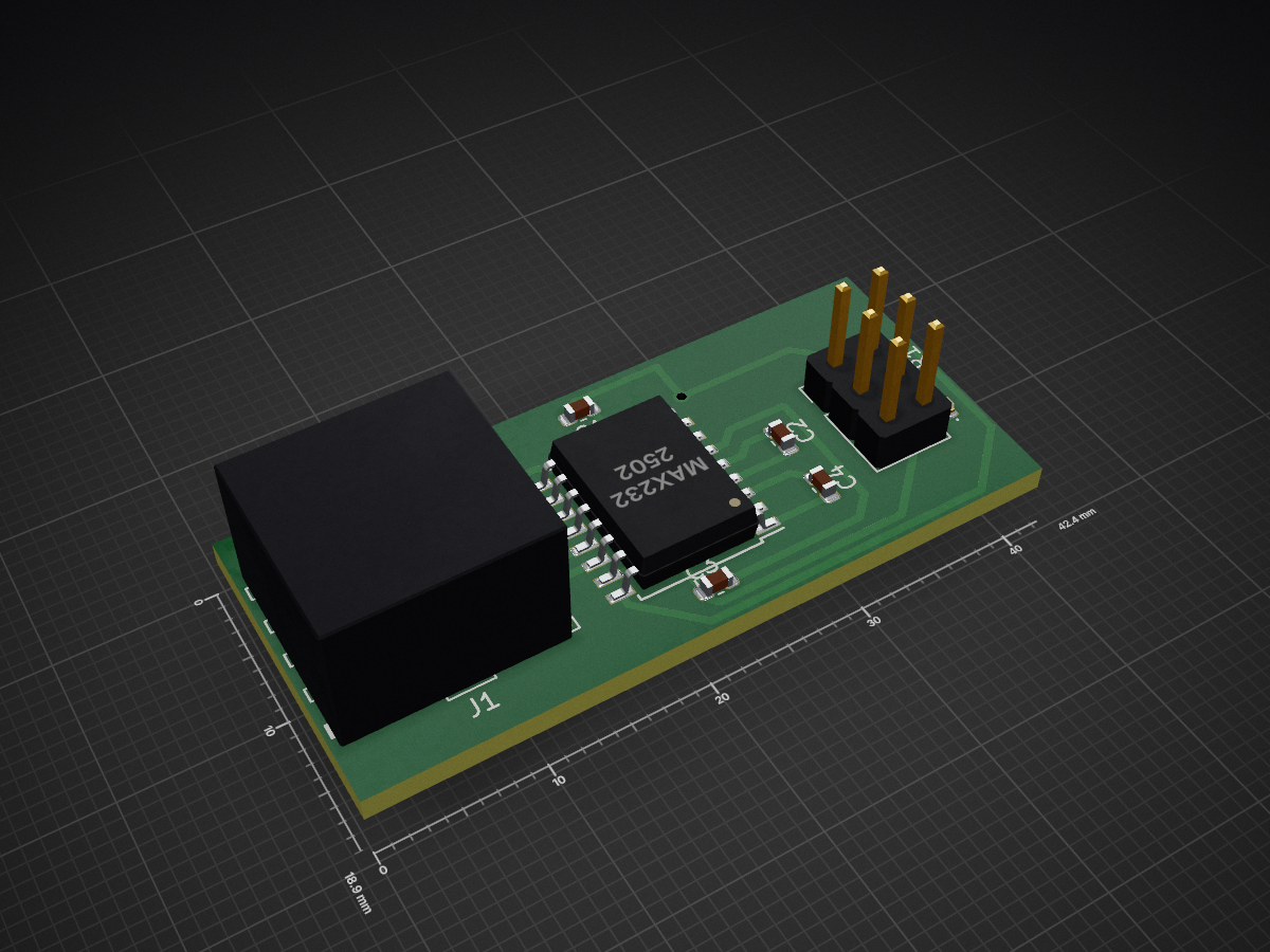
2 layersTiny85 spi controller, the printed circuit board in 3D

Tiny85 spi controller

androiders/pcbs

Rpo for pcb layouts, gerber and gcode files

Copper layers
2
Thickness
1.6 mm
Parts
11
Nets
23
Pads
52
Tracks, vias
107, 4
Routed
Yes
KiCad
KiCad 5 (file 20171130)
Created
18 Jun 2018
Updated
30 Aug 2022

Overview

Tiny85 spi controller is an open-source printed circuit board by androiders, from the androiders/pcbs repository on GitHub. It is a 2-layer board with 11 parts on 23 nets, routed with 107 tracks and 4 vias.

It is built around the ATTINY85V-10SU and MAX232N. Its parts include 4 capacitors, 2 ICs, 2 connectors, 1 resistor and 1 diode. It belongs with the AVR (ATmega, ATtiny) boards of this library.

Main components

2

README

README.md

View this project on CADLAB.io.

pcbs

Repo for pcb layouts, gerber and gcode files

Ki-Cad

PCB layout:

  • Use as wide traces as possible. 1mm preffered.
  • Dont use "filled areas" if possible. It does not make good geometry in flatcam
  • Don't forget to set origin marker
  • Export gerber: use auxiliary axis

FlatCam

geometry generation:

  • If you are using thru-hole components or using bottom layer, mirror around y axis for both geometry and Drilling
  • Edit drill files if necessary for fewer drill sizes
  • TODO: test double sided layout by mirroring around center axis!

Isolation generation:

  • Current isolation mill depth to test: 0.04 mm (0.05 was tested and seems to work fine!) (Common copper depth is about 0.03 mm)

  • Current feedrate on isolation milling to test: 60 mm/s

  • spindle speed 12000 rpm

  • use 0.2 mm tool width on cnc generation

  • 2 passes with 0.1 overlap

Cutout generation:

  • Current cutout mill depth: 1.6 mm
  • Current feedrate on cutout milling: 40 mm/s
  • spindle speed 12000 rpm

FlatCam defaults:

  • put a link in ~/.FlatCAM/defaults.json

bCNC

Probe:

  • Fastfeed: 120
  • Probefeed: 25
  • Probe points: 4/cm (in each direction)

Drilling:

  • Current drill plunge rate to test 20 mm/s
  • spindle speed: 12000 rpm
  • Drill depth: 1.6

Parts

11
QtyValueFootprintReferences
4CCapacitor_SMD:C_0603_1608MetricC1, C2, C3, C4
1ATtiny85V-10SUPackage_SO:SOIJ-8_5.3x5.3mm_P1.27mmU2
1ISPConnector_PinHeader_2.54mm:PinHeader_2x03_P2.54mm_VerticalJ3
1LEDLED_SMD:LED_0402_1005MetricD1
1MAX232Package_SO:SOIC-16W_7.5x10.3mm_P1.27mmU1
1RResistor_SMD:R_0201_0603MetricR1
1SW_PushButton_Switch_SMD:SW_SPST_CK_RS282G05A3SW1
1rs232Connector_Harwin:Harwin_M20-89005xx_1x05_P2.54mm_HorizontalJ1

Questions

What parts does the Tiny85 spi controller use?

11 parts, built around the ATTINY85V-10SU and MAX232N. The full list of its parts is on this page, with links to each part's symbol and footprint where PCBKit's library has them.

Where can I download the Tiny85 spi controller KiCad files?

From the androiders/pcbs repository on GitHub, at the commit this page was made from: the board is tiny85 spi controller/tiny85 spi controller.kicad_pcb. PCBKit opens the board in the browser, with nothing to install.

Can I use the Tiny85 spi controller design in my own project?

Its repository states no licence, so its author keeps all rights: ask androiders before reusing the design.

More from androiders/pcbs

12
  • 2 layers58 × 80 mmMc unit, the printed circuit board in 3D

    Mc unit

    androiders/pcbs

    Rpo for pcb layouts, gerber and gcode files

    54 parts
  • 2 layersBrewer, the printed circuit board in 3D

    Brewer

    androiders/pcbs

    Rpo for pcb layouts, gerber and gcode files

    33 parts
  • 2 layersThis might work, the printed circuit board in 3D

    This might work

    androiders/pcbs

    Rpo for pcb layouts, gerber and gcode files

    30 parts
  • 2 layersSignalbuffer, the printed circuit board in 3D

    Signalbuffer

    androiders/pcbs

    Rpo for pcb layouts, gerber and gcode files

    28 parts
  • 2 layers65.3 × 48.5 mmDistpedal, the printed circuit board in 3D

    Distpedal

    androiders/pcbs

    Rpo for pcb layouts, gerber and gcode files

    27 parts
  • 2 layersH bridge, the printed circuit board in 3D

    H bridge

    androiders/pcbs

    Rpo for pcb layouts, gerber and gcode files

    20 parts
  • 2 layersSmps, the printed circuit board in 3D

    Smps

    androiders/pcbs

    Rpo for pcb layouts, gerber and gcode files

    18 parts
  • 2 layers44 × 50 mmH bridge-2, the printed circuit board in 3D

    H bridge-2

    androiders/pcbs

    Rpo for pcb layouts, gerber and gcode files

    17 parts
  • 2 layers73.7 × 34.3 mmMicpreamp, the printed circuit board in 3D

    Micpreamp

    androiders/pcbs

    Rpo for pcb layouts, gerber and gcode files

    17 parts
  • 2 layersSignalbuffer single, the printed circuit board in 3D

    Signalbuffer single

    androiders/pcbs

    Rpo for pcb layouts, gerber and gcode files

    14 parts
  • 2 layersAtmega8breakeout, the printed circuit board in 3D

    Atmega8breakeout

    androiders/pcbs

    Rpo for pcb layouts, gerber and gcode files

    12 parts

Similar boards

  • 2 layers15.3 × 19.3 mmKicad hx711 tyny85, the printed circuit board in 3D

    Kicad hx711 tyny85

    IvDm/Z-probe-on-smd-resistors-2512

    Auto bed level strain gage for 3D printer using resistors 2512 instead of strain gauges.

    18 parts150GPL-3.0
  • 4 layers110.7 × 69.8 mmSgb mbc5 1-4, the printed circuit board in 3D

    Sgb mbc5 1-4

    MouseBiteLabs/Super-Game-Boy-Plus

    A replacement circuit board for improving the Super Game Boy, or for creating a standalone Game Boy game for the SNES.

    95 parts41CC-BY-SA-4.0
  • 2 layers12.2 × 40.4 mmBadUSB, the printed circuit board in 3D

    BadUSB

    joelsernamoreno/Attiny85-Standalone

    PCB designs based on the Attiny85 microcontroller for standalone development.

    7 parts21CC-BY-4.0
  • 2 layers34 × 12.2 mmSpherometer display, the printed circuit board in 3D

    Spherometer display

    hzeller/digi-spherometer

    A digital spherometer, reading data from digital dial indicator and converting it to radius, displaying on OLED display.

    14 parts14GPL-3.0
  • 2 layers72.7 × 114 mmWs 3.0, the printed circuit board in 3D

    Ws 3.0

    boanjo/myhome

    A collection of mysensors nodes, gateways and HW from my home

    57 parts4
  • 2 layers54 × 29 mmSonos magic hub, the printed circuit board in 3D

    Sonos magic hub

    perja12/sonos_magic_hub

    Circuit for using the LG OLED C9 TV remote (LG Magic Remote) with the Sonos Playbar.

    18 parts3Apache-2.0
  • 2 layers16 × 110 mmGatekeeper, the printed circuit board in 3D

    Gatekeeper

    mjrskiles/gatekeeper

    A digital gate/trigger processor for Eurorack modular synthesizers. Gatekeeper has a two-state (0 or 5V) output driven by push button and CV input. The input response is configurable via menu settings.

    33 parts2MIT
  • 2 layers19.6 × 24.1 mmMoleblink, the printed circuit board in 3D

    Moleblink

    rjhsun/moleblink

    ATtiny85-based illuminated PCB keychain featuring the Blacker House crest

    31 parts2CC-BY-SA-4.0