
4 layers100 × 79 mm

 rjhsun/moleblink2
ATtiny85-based illuminated PCB keychain featuring the Blacker House crest
Moleblink is an open-source printed circuit board by rjhsun, from the rjhsun/moleblink repository on GitHub, published under the CC-BY-SA-4.0 licence. It is a 2-layer board of 19.6 × 24.1 mm with 31 parts on 33 nets, routed with 206 tracks and 10 vias.
It is built around the ATTINY85V-10SU, 74HC595 and 150120BS75000, with the 0ZCJ0005FF2E, IRFML8244TR and JS202011JCQN among its other parts. Its parts include 11 resistors, 8 diodes, 2 capacitors, 2 ICs and 2 switches. It belongs with the AVR (ATmega, ATtiny) boards of this library.



ATtiny85-based illuminated PCB keychain featuring the Blacker Hovse crest
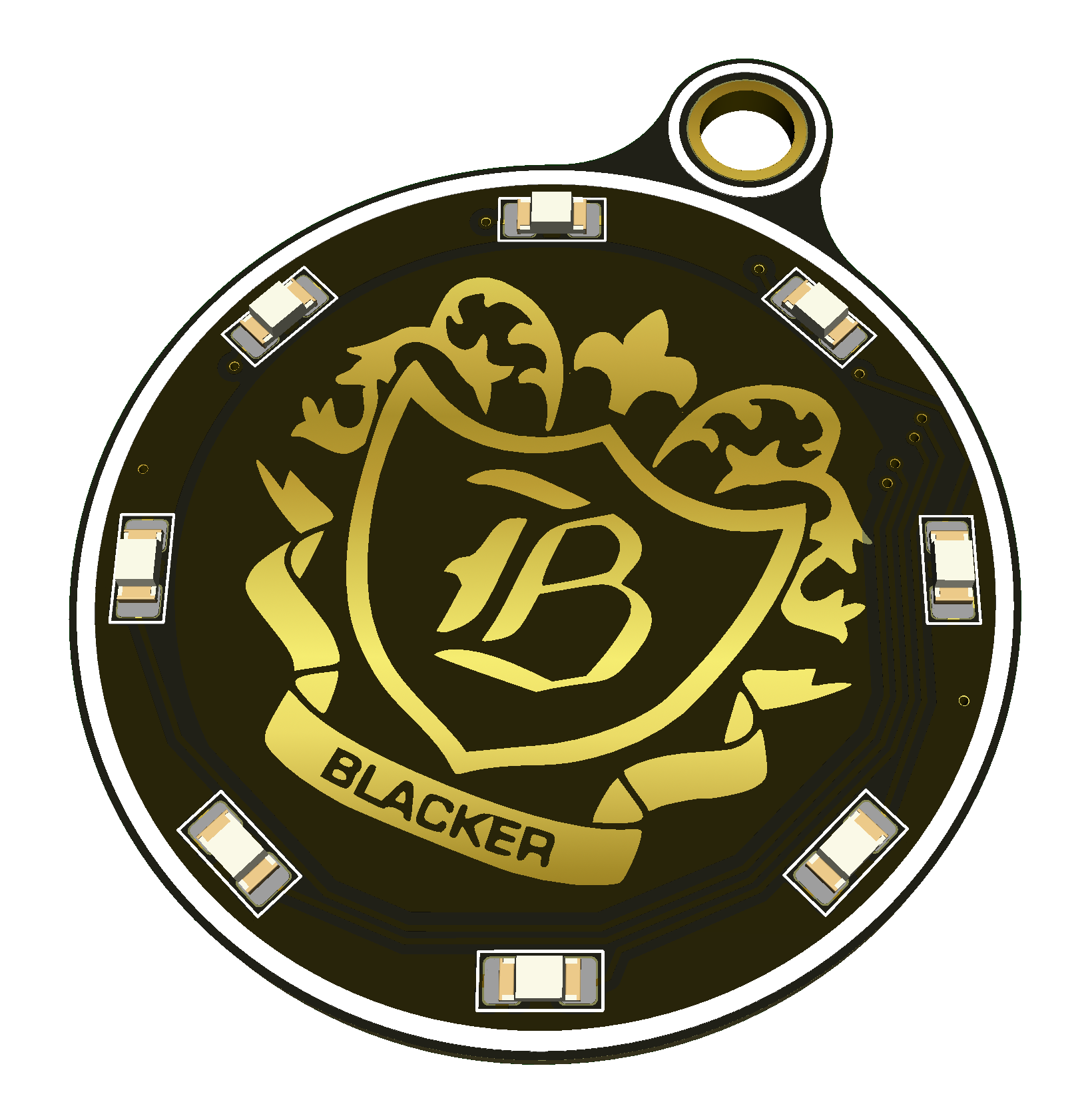
Blacker Hovse (House) is one of the eight student houses in the undergraduate housing system at Caltech. Blacker was founded in 1932 and named after Robert Roe Blacker, a trustee of Caltech. Notable alumni from Blacker include William Shockley, Walter Munk, Carver Mead, and Kip Thorne. The current house motto is Sed nvlla nisi ardva virtvs.
This is a 1.6" by 1.9" PCB keychain featuring the Blacker Hovse crest on the top copper, based on RuddBlink. A ring of 8 LEDs around the crest is controlled by an ATtiny85 through a 74HC595 shift register. This keychain is intended to be compact and aesthetic, but also simple to solder; all packages are SOIC and 0805 or larger.
The keychain can be powered by a single CR2032 coin cell through the coin cell holder footprint on the back, or through an alternative power source soldered to those pads.
No input voltage regulation is present. Do not apply more than 5.5 V, the maximum voltage for the ATtiny.
This PCB is designed with KiCad EDA 5.1.4. Schematic and board files may be found under /moleblink, with documentation under /moleblink/doc.

Unless otherwise noted, this schematic and PCB design, with associated symbol and footprint files, are licensed under a Creative Commons Attribution-ShareAlike 4.0 International License.
| Qty | Value | Footprint | References |
|---|---|---|---|
| 8 | 150120BS75000 | ruddblink:LED_1206_Uniform_HandSolder | D1, D2, D3, D4, D5, D6, D7, D8 |
| 8 | R | Resistor_SMD:R_0805_2012Metric_Pad1.15x1.40mm_HandSolder | R1, R2, R3, R4, R5, R6, R7, R8 |
| 3 | 10K | Resistor_SMD:R_0805_2012Metric_Pad1.15x1.40mm_HandSolder | R9, R10, R11 |
| 2 | 0.1uF | Capacitor_SMD:C_0805_2012Metric_Pad1.15x1.40mm_HandSolder | C1, C2 |
| 1 | 0ZCJ0005FF2E | Fuse:Fuse_1206_3216Metric_Pad1.42x1.75mm_HandSolder | F1 |
| 1 | IRFML8244 | Package_TO_SOT_SMD:SOT-23_Handsoldering | Q1 |
| 1 | 3034 | ruddblink:BatteryHolder_Keystone_3034_Wide | BT1 |
| 1 | 74HC595 | Package_SO:SOIC-16_3.9x9.9mm_P1.27mm | U2 |
| 1 | ATtiny85V-10SU | Package_SO:SOIJ-8_5.3x5.3mm_P1.27mm | U1 |
| 1 | JS202011JCQN | ruddblink:SW_SPDT_CK-JS202011JCQN | SW1 |
| 1 | KEYHOLE | ruddblink:MountingHole_Keyring | H1 |
| 1 | LOGO | crest:blacker_mask | G*** |
| 1 | LOGO | ruddblink:OSHW-Symbol_140mil | G*** |
| 1 | PTS526 SK15 SMTR2 LFS | ruddblink:SW_Push_PTS526 | SW2 |

kajusK/Pneumobil
Control and telemetry system for BUT Falcon pneumobil for Aventics Pneumobil competition


It measures 19.6 × 24.1 mm and has 2 copper layers, 1.6 mm thick.
31 parts, built around the ATTINY85V-10SU, 74HC595, 150120BS75000 and 0ZCJ0005FF2E. The full list of its parts is on this page, with links to each part's symbol and footprint where PCBKit's library has them.
From the rjhsun/moleblink repository on GitHub, at the commit this page was made from: the board is moleblink/moleblink.kicad_pcb. PCBKit opens the board in the browser, with nothing to install.
Its repository publishes it under the CC-BY-SA-4.0 licence: you may reuse it on that licence's terms (keep the author's notice, and for a copyleft licence share your changes alike).