2 layers21.1 × 45.7 mm
RP2040-base example
TT-392/RP2040-base-example
Revision 0.9 was produced at jlcpcb. The rev number was bumped to 1.0 after the pcb was tested. There were no changes between rev 0.9 and 1.0.
34 parts

 TT-392/playstation_adapter_pcb
I only wrote software for the Taiko drum, but in theory, all of the hardware is there to support a lot of different kinds of PlayStation controllers. The firmware can be found here.
Playstation adapter is an open-source printed circuit board by TT-392, from the TT-392/playstation_adapter_pcb repository on GitHub. It is a 2-layer board of 26.1 × 56.7 mm with 39 parts on 57 nets, routed with 375 tracks and 50 vias.
It is built around the RP2040, AMS1117-3.3 and SRV05-4, with the GT-USB-7047C and X322512MSB4SI among its other parts. Its parts include 18 capacitors, 10 resistors, 4 ICs, 4 connectors and 1 switch. It belongs with the interfaces and adapters boards and the RP2040 boards of this library.


This project is a simple PlayStation 1/2 controller port to USB C adapter. I made it so that I would be able to use it with the cheap, second hand, PlayStation 2, Taiko no Tatsujin drum, which I bought while in Japan.
I only wrote software for the Taiko drum, but in theory, all of the hardware is there to support a lot of different kinds of PlayStation controllers. The firmware can be found here.
If you want to use this hardware with other PlayStation controllers, you are going to have to write your own firmware. For details on how to do this, I recommend the following source: Interfacing a PS2 (PlayStation 2) Controller.
One thing to keep in mind is power requirements of the controller you are using. I haven't found much information on how much power controllers pull (not that I put in that much effort), except for what is mentioned in the aforementioned source. Therefore, I can only give information on the power supply situation of this PCB.
I used JLCPCB to order my PCBs with all of their parts already pick and placed. I used this plugin to do this. However, if you just want to order the same PCBs as I did, without any modifications, you can just grab the production files from the "JLCPCB" folder, or from the "releases" tab on github. The rest of this guide assumes you have your PCBs with the SMD components fully assembled at JLCPCB (nothing is stopping you from soldering them on yourself of course).
Apart from the PCBs, you should get your hands on some PlayStation controller ports with 90 degree pins. I got mine from AliExpress (AliExpress links rot quickly, but you should be able to find something similar). And some 9 pin, 3.96mm pitch pin header, I used these (At the time of writing, you get free shipping on LCSC, if your recently ordered something from JLCPCB). And if you want some protection for your board, get some 50mm diameter heat-shrink (I got this stuff from AliExpress, seems to work well).
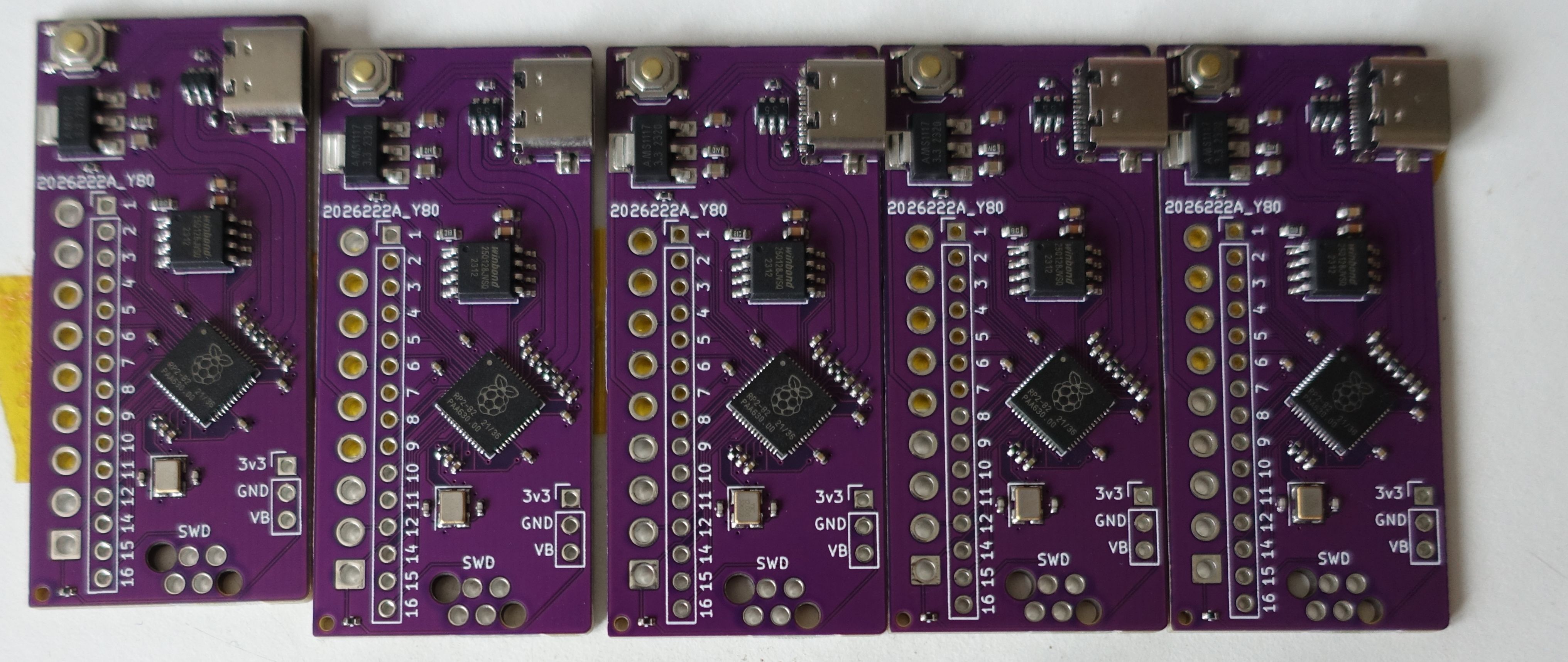
If you followed the ordering instructions, you should now have a PCB that looks something like one of these:
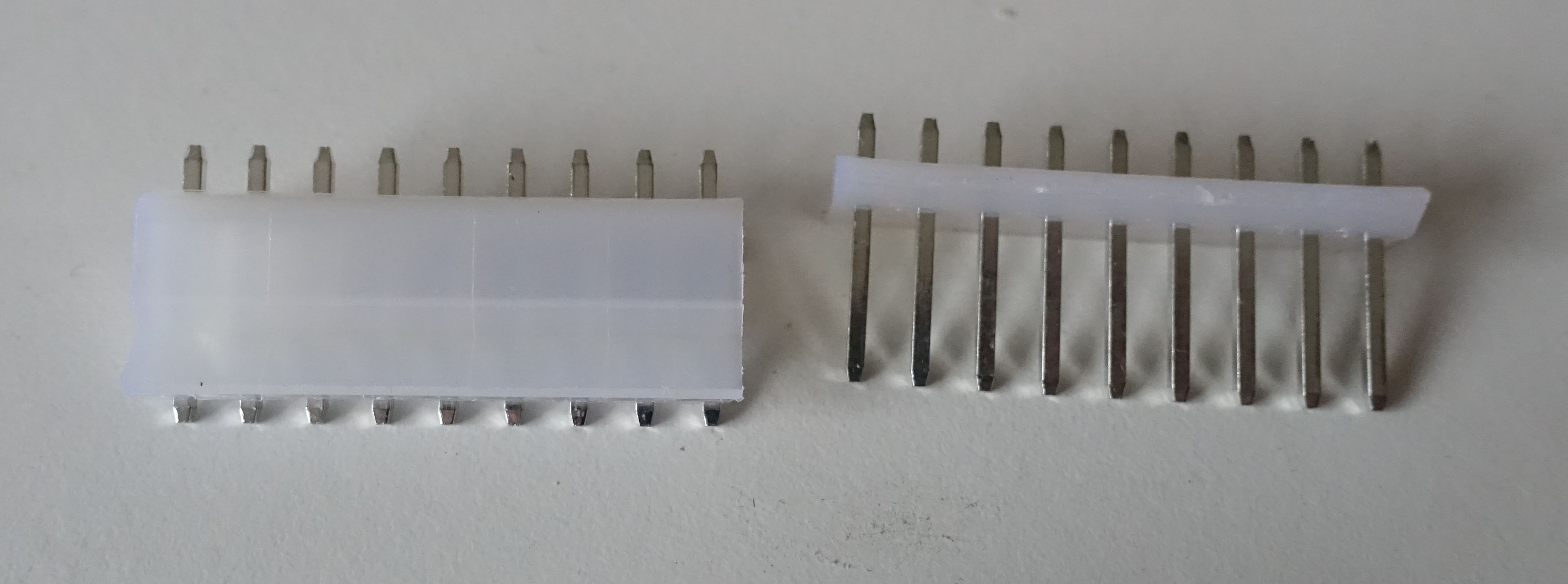
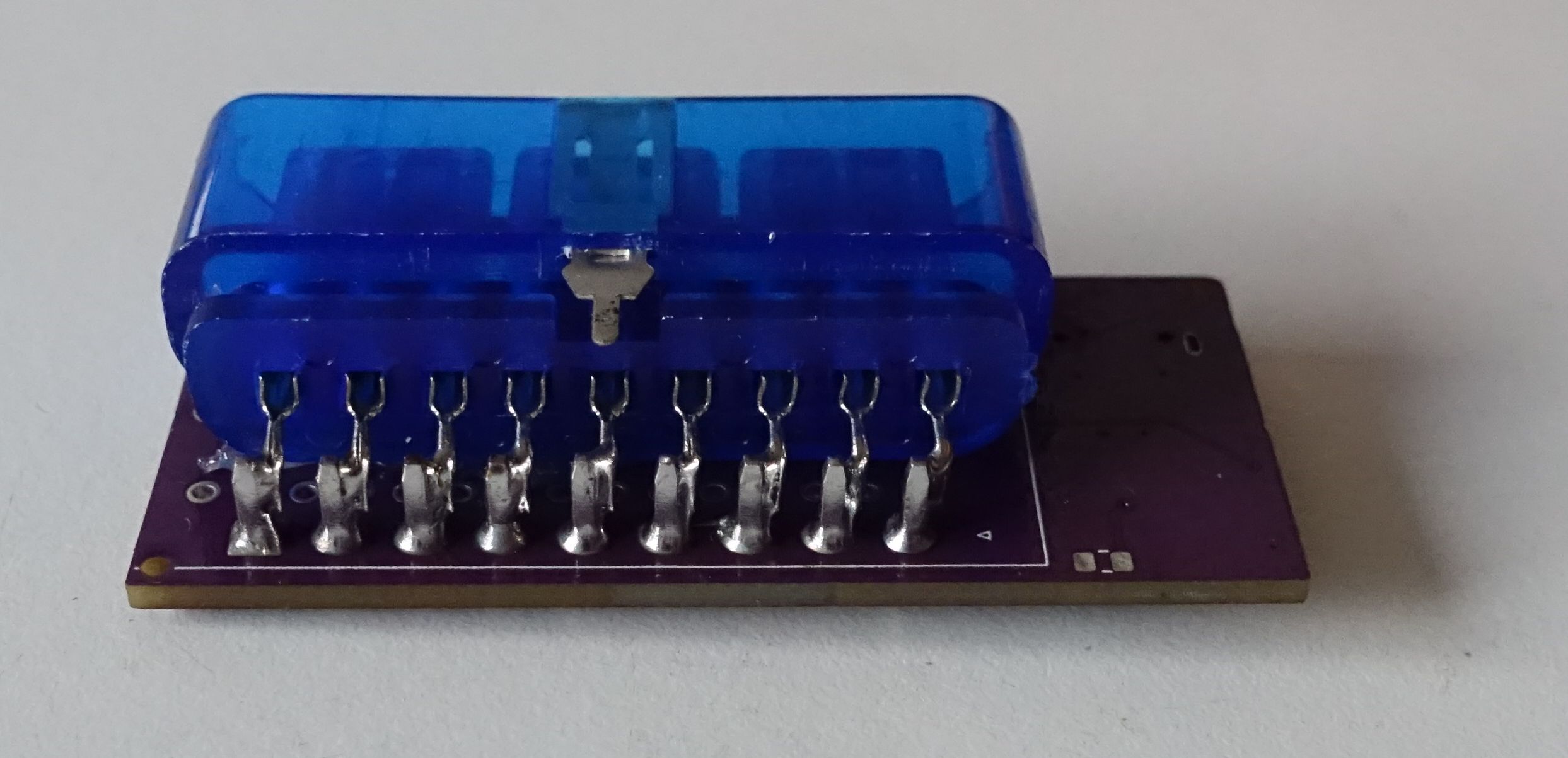
Because the 90 degree PlayStation ports don't quite reach to the PCB, a we need something to bridge the gap. To do this, I decided to use some 3.96mm pitch, 9 pin pin headers, sadly, I couldn't find any without a plastic tab, so I just got the ones that looked like they had a tab that was easy to remove. So that is the first step in assembly, remove this tab, like is shown in the following image:
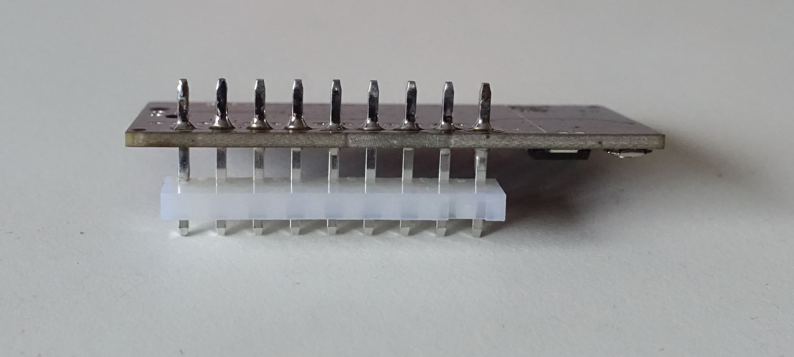
Next, this header should be soldered to the PCB, I have found that it works best if you solder on the connector with the pins sticking out about 5 mm, and with the side of the connector that has the least plastic, pointing to the edge of the board, to allow for easier snipping later (I found out about this orientation trick in the next one I assembled, therefore the pictures have the connector rotated by 180 degrees compared to what I am saying here).
Next, we glue (I used hot glue) the connector to the bottom side of the PCB, with the pins as close as possible to the pin header's pins, like shown in the following picture
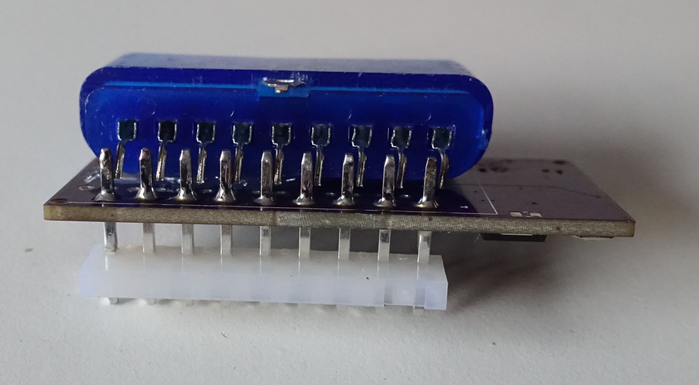
The next step is to solder these pins together, be sure to use ample solder, to make sure the pins really have a good connection.
After you have soldered these pins together, you can go ahead and use some side cutters to cut the pins of the connector on the other side of the board. The result of these two steps can be seen in the following image:
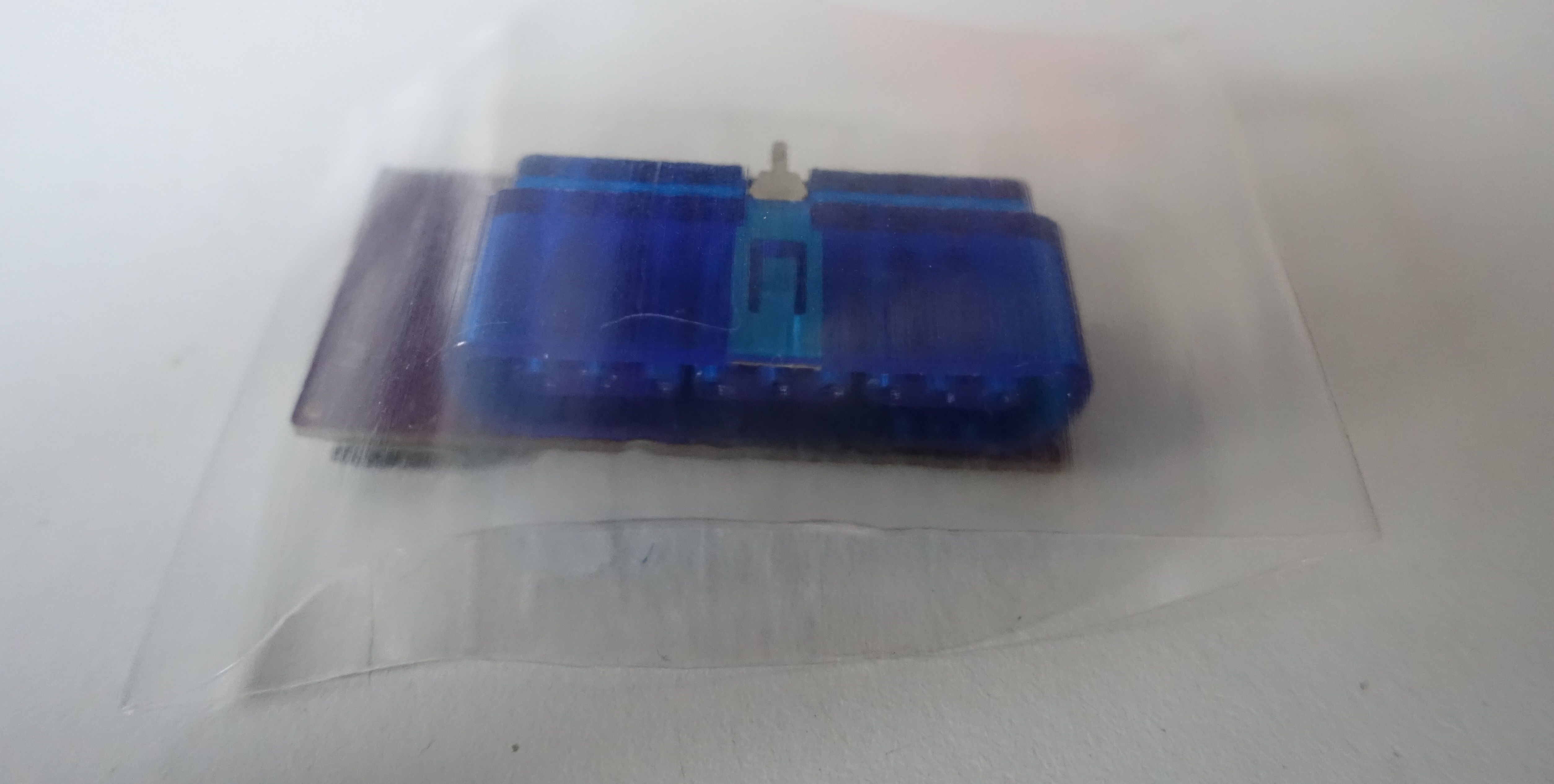
Now it is time to heat shrink our adapter for some extra protection. Cut off a decent size piece of the heat shrink, so that the adapter can sit inside, with ample space on both sides:
Now use a heat gun to shrink the heat-shrink:
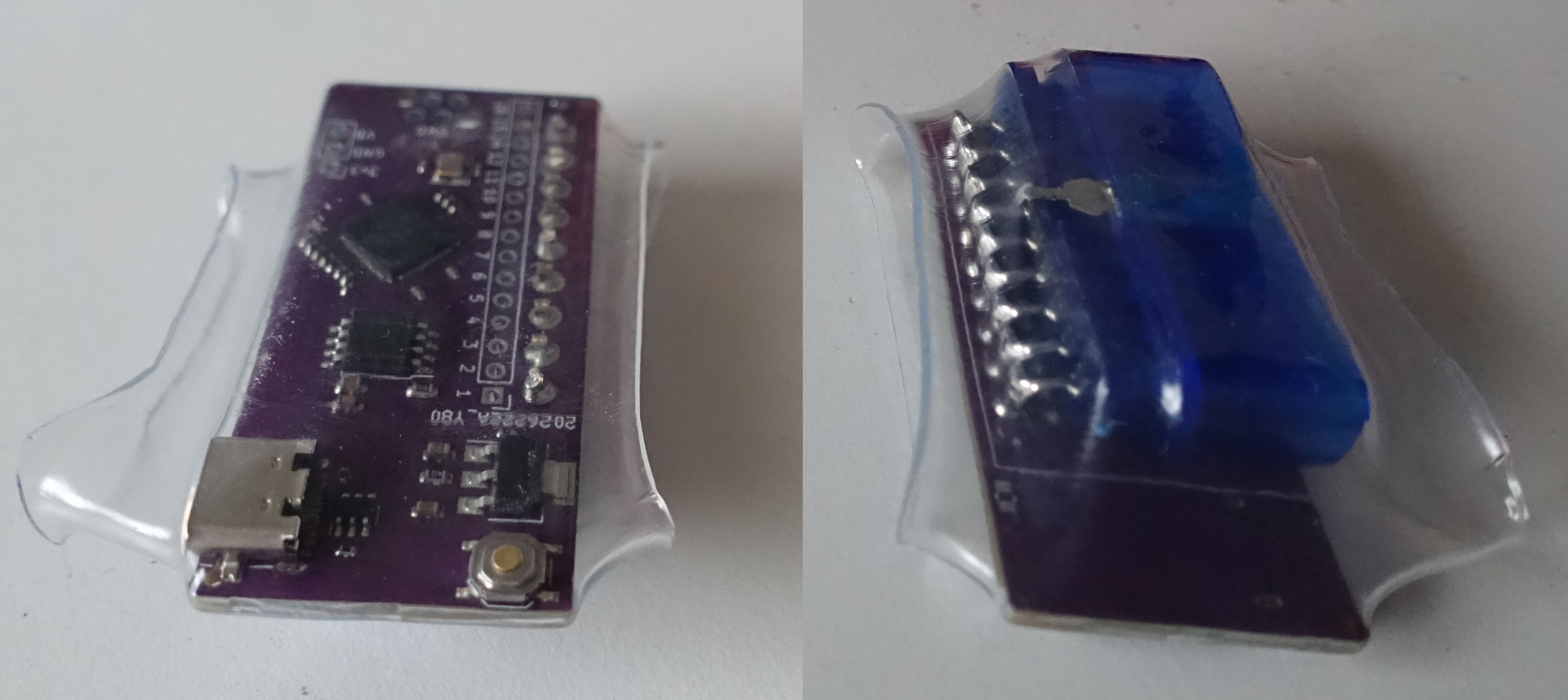
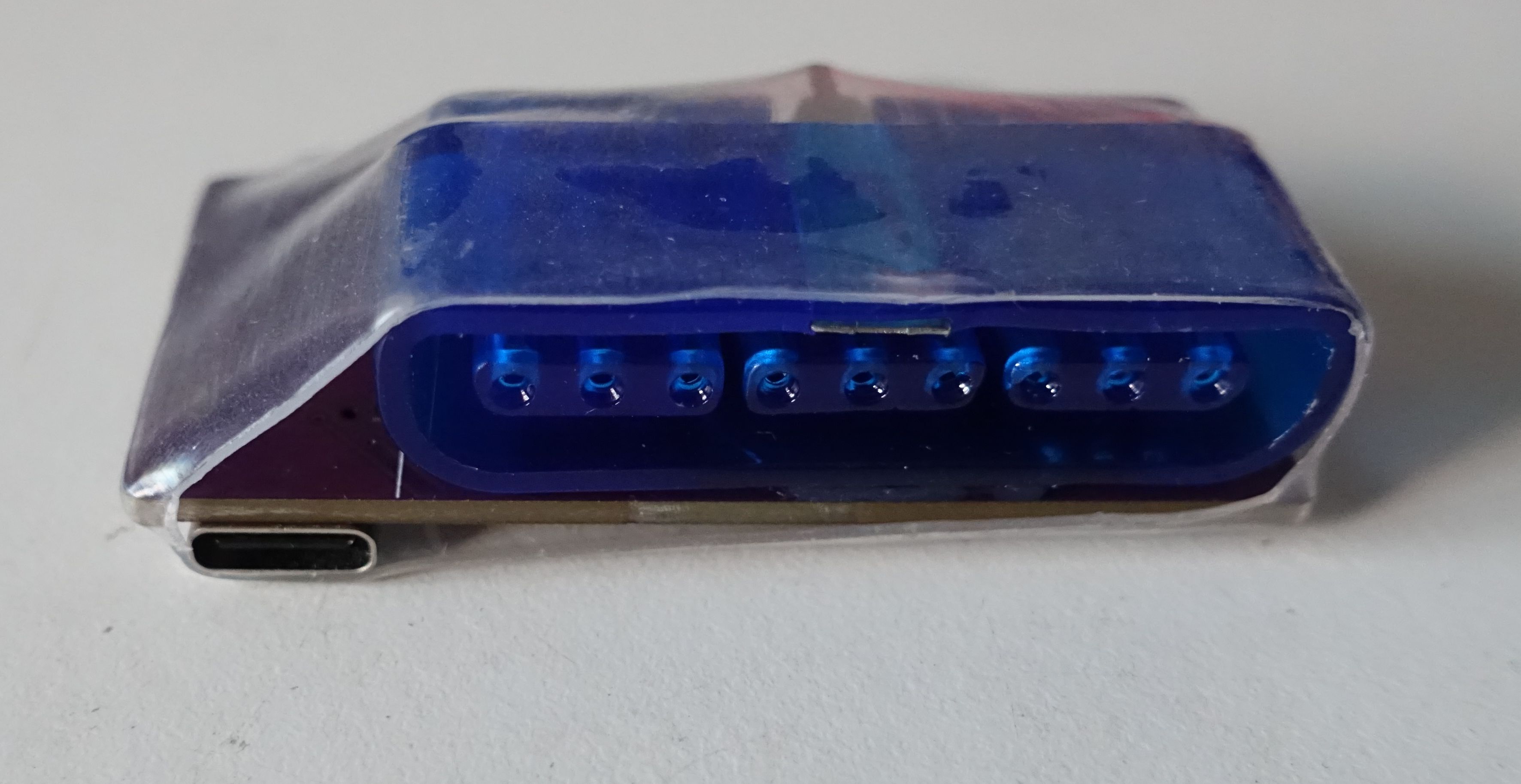
Now we can cut away the excess heat-shrink (I used normal scissors, just make sure they are scissors that close well), and we have our finished adapter:
| Qty | Value | Footprint | References |
|---|---|---|---|
| 10 | 100n | Capacitor_SMD:C_0402_1005Metric | C3, C4, C5, C6, C7, C8, C9, C10, C11, C12 |
| 2 | 1k5 | Resistor_SMD:R_0402_1005Metric | R9, R10 |
| 2 | 1u | Capacitor_SMD:C_0402_1005Metric | C13, C14 |
| 2 | 27 | Resistor_SMD:R_0402_1005Metric | R3, R4 |
| 2 | 30p | Capacitor_SMD:C_0402_1005Metric | C15, C16 |
| 2 | 5k1 | Resistor_SMD:R_0402_1005Metric | R7, R8 |
| 1 | 0, DNF | Resistor_SMD:R_0805_2012Metric | R2 |
| 1 | 100n | Capacitor_SMD:C_0603_1608Metric | C17 |
| 1 | 10n | Capacitor_SMD:C_0603_1608Metric | C18 |
| 1 | 1R | Resistor_SMD:R_0603_1608Metric | R1 |
| 1 | 1k | Resistor_SMD:R_0402_1005Metric | R5 |
| 1 | 1k | Resistor_SMD:R_0603_1608Metric | R6 |
| 1 | 1u | Capacitor_SMD:C_0603_1608Metric | C1 |
| 1 | 22u | Capacitor_SMD:C_0603_1608Metric | C2 |
| 1 | AMS1117-3.3 | footprints:SOT-223-3_TabPin2_flipped_for_jlcpcb | U1 |
| 1 | Conn_01x03 | Connector_PinHeader_2.54mm:PinHeader_1x03_P2.54mm_Vertical | J1 |
| 1 | Conn_01x04 | footprints:REDFIT 4 pin | SWD1 |
| 1 | Conn_01x13 | footprints:PinHeader_1x15_P2.54mm_Vertical_no_courtyard | J2 |
| 1 | GT-USB-7047C | footprints:GT-USB-7047C | J3 |
| 1 | RP2040 | Package_DFN_QFN:QFN-56-1EP_7x7mm_P0.4mm_EP3.2x3.2mm | U3 |
| 1 | SRV05-4 | footprints:SOT-23-6_flipped_for_jlcpcb | U2 |
| 1 | SW_Push | RP2040_base:TS-1187A | SW1 |
| 1 | W25QXXXJV | RP2040_base:SOIC-8_5.275x5.275mm_P1.27mm | U4 |
| 1 | X322512MSB4SI | RP2040_base:YSX321SL, datasheet recommended measurements | Y1 |
| 1 | ~ | footprints:PSX port | J4 |
TT-392/RP2040-base-example
Revision 0.9 was produced at jlcpcb. The rev number was bumped to 1.0 after the pcb was tested. There were no changes between rev 0.9 and 1.0.


janelia-kicad/cluster-pcb
PCB for each cluster of prisms in the Voigts Lab honeycomb maze.


cosmosalad/Gear80
Gear80 is a 80% keyboard based on the rp2040.


cosmosalad/Gear60
Gear60 is a 60% multi-layout keyboard based on the rp2040.
It measures 26.1 × 56.7 mm and has 2 copper layers, 1.6 mm thick.
39 parts, built around the RP2040, AMS1117-3.3, SRV05-4 and GT-USB-7047C. The full list of its parts is on this page, with links to each part's symbol and footprint where PCBKit's library has them.
From the TT-392/playstation_adapter_pcb repository on GitHub, at the commit this page was made from: the board is playstation_adapter.kicad_pcb and its schematic RP2040-base/RP2040_base.kicad_sch. PCBKit opens the board in the browser, with nothing to install.
Its repository states no licence, so its author keeps all rights: ask TT-392 before reusing the design.