2 layers40 × 40 mm

 janelia-kicad/cluster-pcb
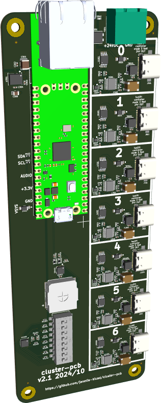
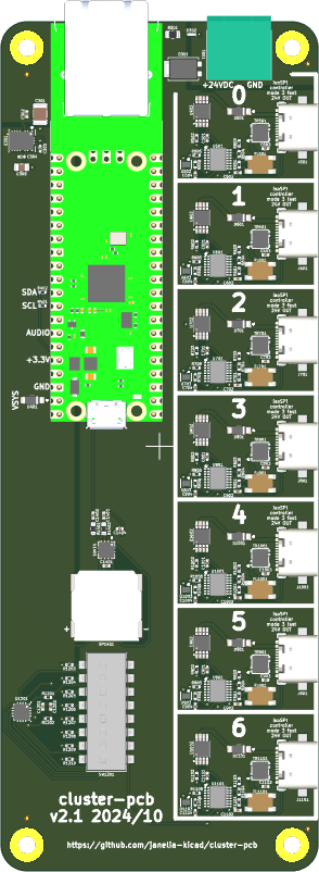
PCB for each cluster of prisms in the Voigts Lab honeycomb maze.
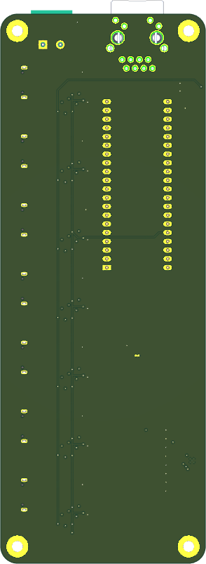
Cluster pcb is an open-source printed circuit board by janelia-kicad, from the janelia-kicad/cluster-pcb repository on GitHub. It is a 4-layer board of 60 × 160 mm with 163 parts on 206 nets, routed with 1,403 tracks and 98 vias.
It is built around the SN74LVC1G125DRYR(UMW), TPSM365R6V5RDNR and LTC6820HMS#3ZZTRPBF, with the TPA6204A1DRBR, TPS1H200AQDGNRQ1 and ERJ2GEJ182X among its other parts. Its parts include 57 resistors, 39 capacitors, 24 ICs, 10 diodes and 7 connectors. It belongs with the RP2040 boards of this library.


[blocked]
[blocked]
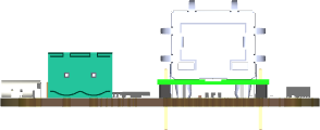


[blocked]
./documentation/schematic/cluster-pcb.pdf
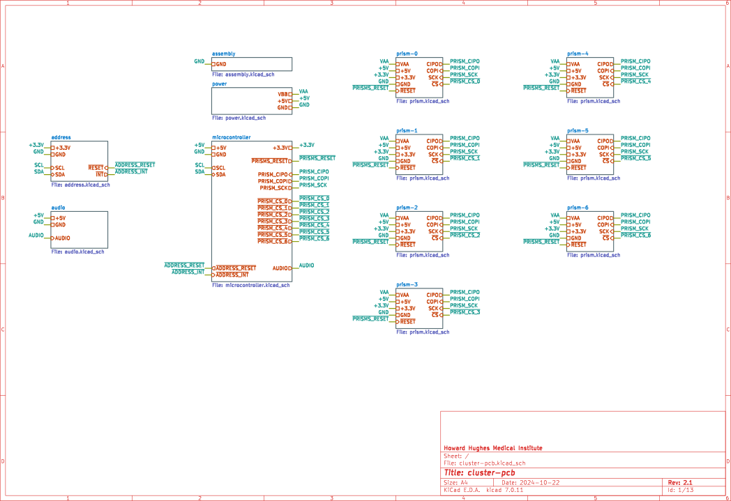
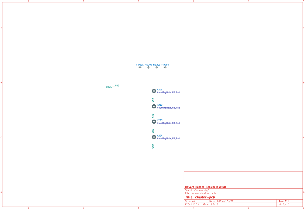
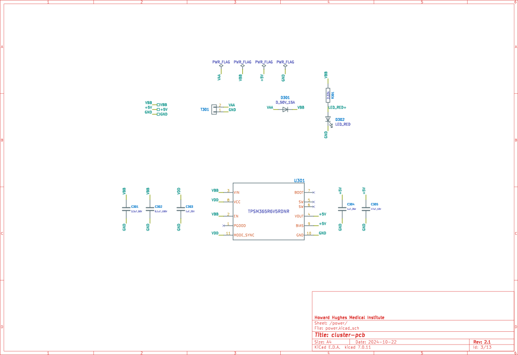
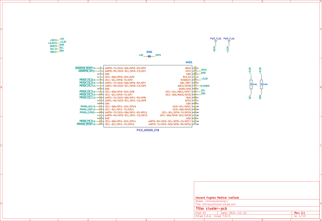
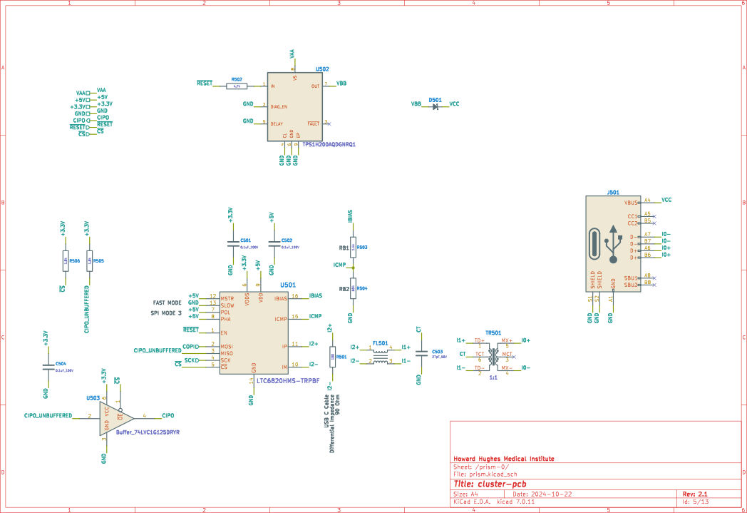
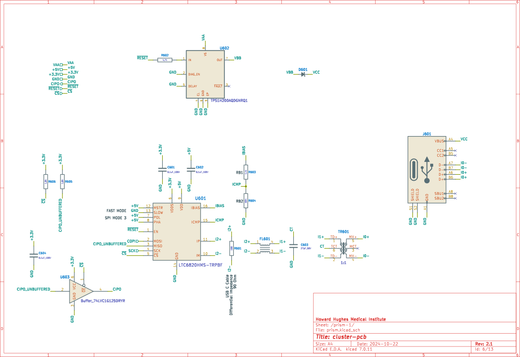
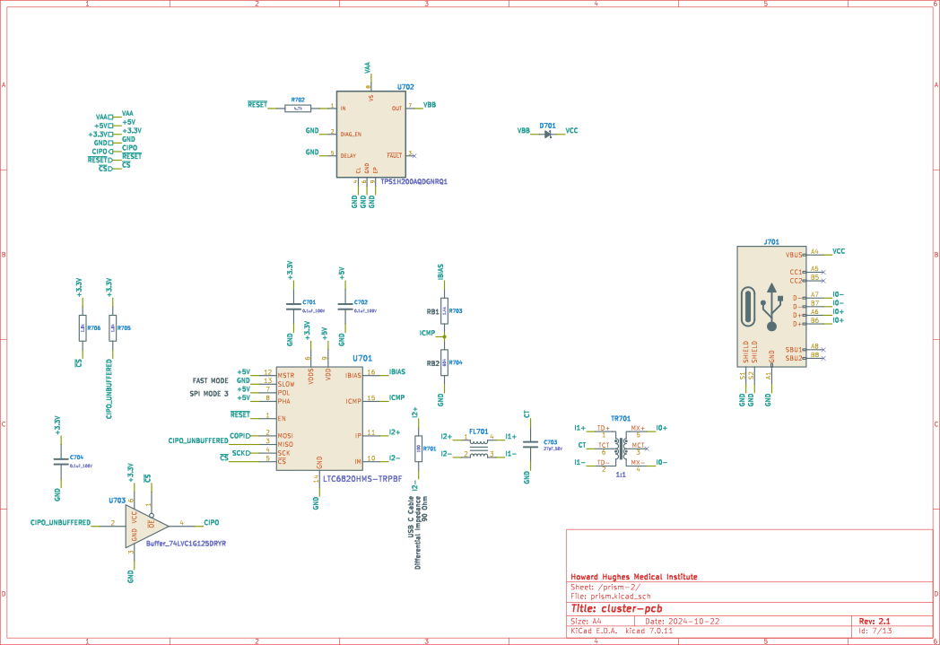
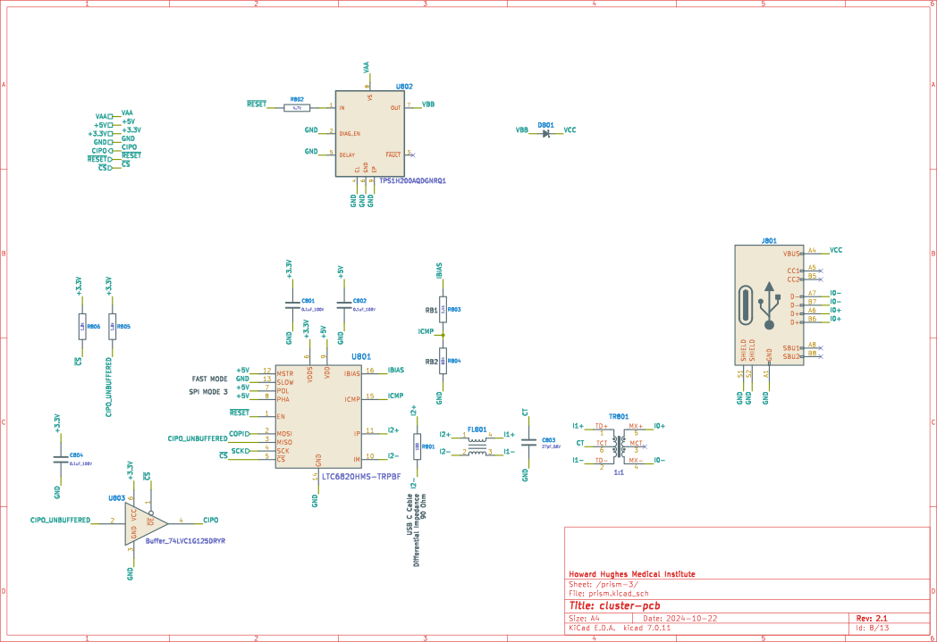
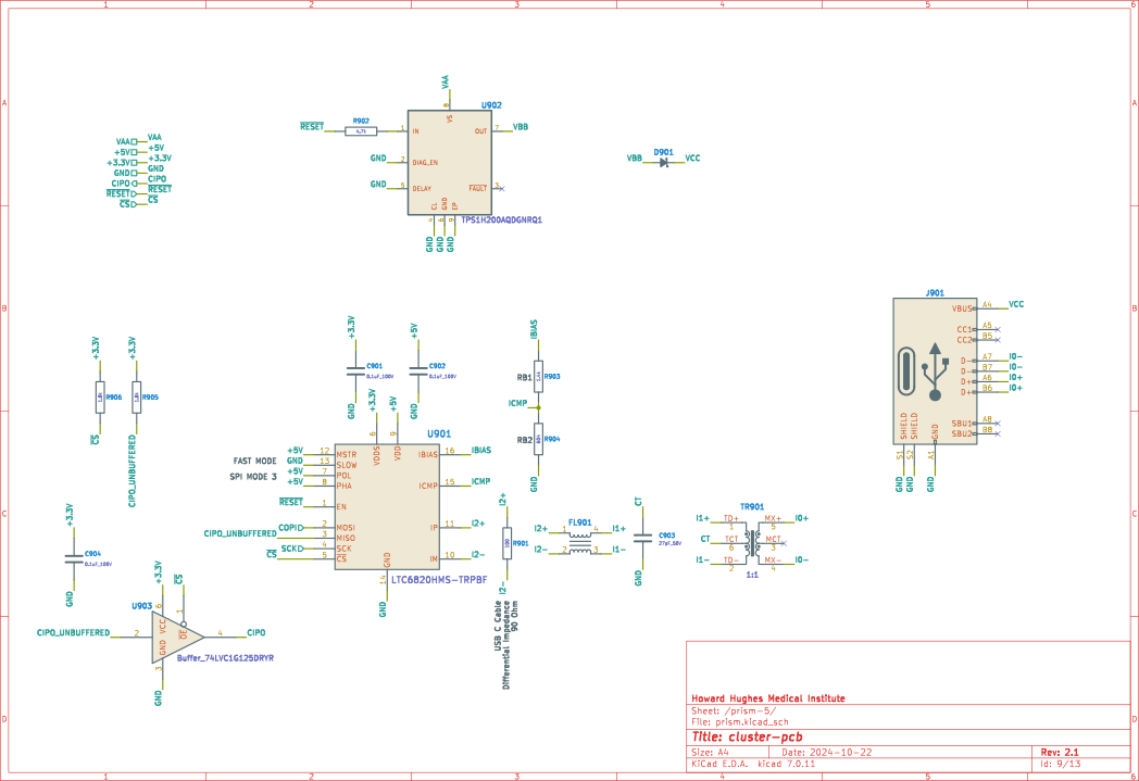
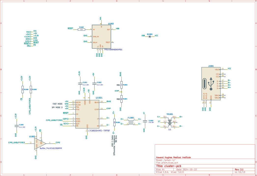
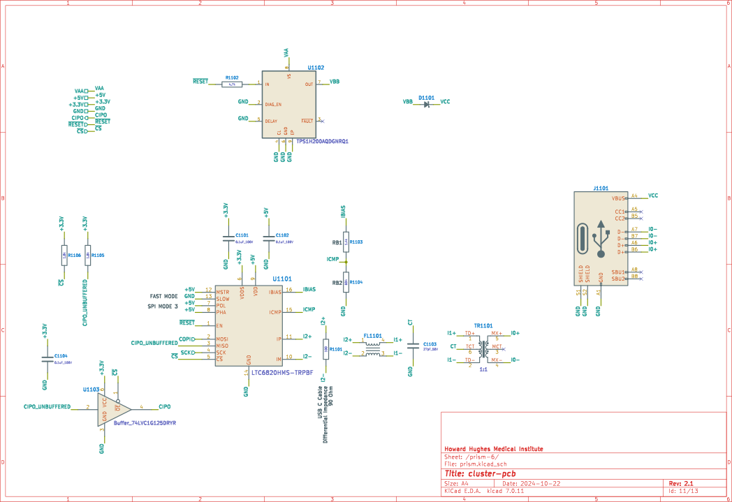
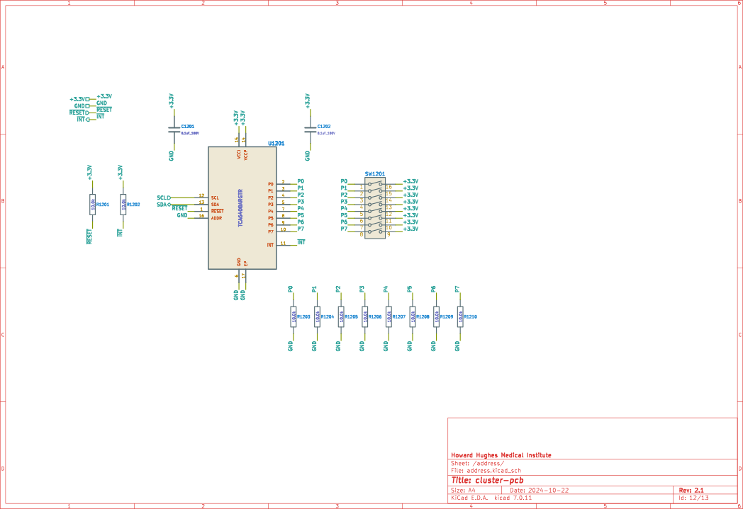
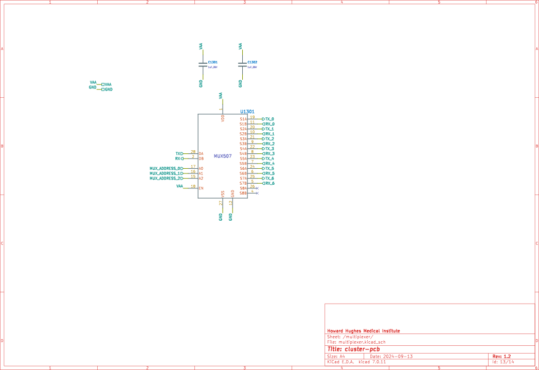
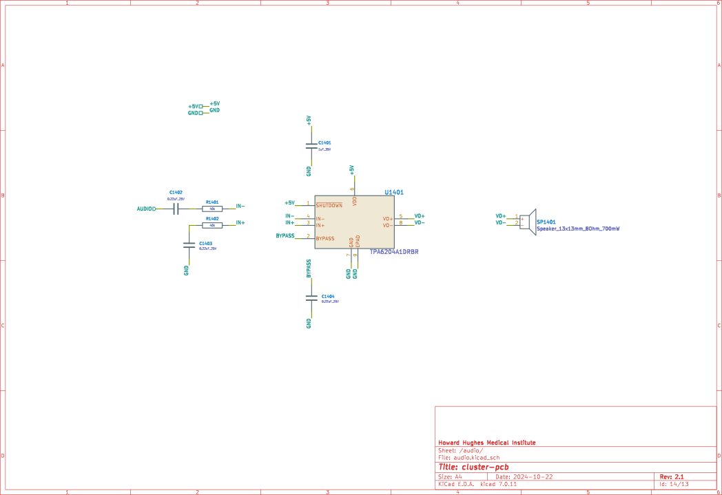
[blocked]
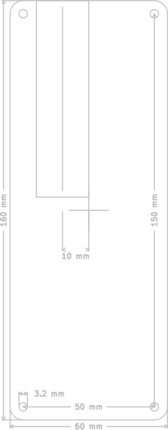
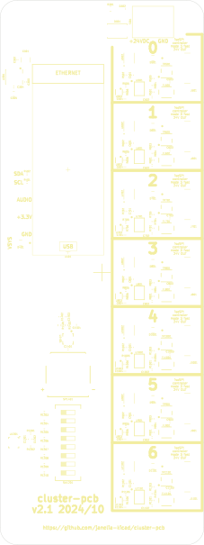

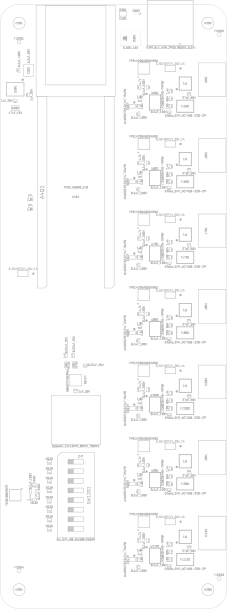

[blocked]
| Item | Synopsis | Manufacturer Part Number | Manufacturer | Quantity | Reference(s) | Package |
|---|---|---|---|---|---|---|
| 1 | 50V 3.3uF | FS32X335K500EGG | PSA(Prosperity Dielectrics) | 1 | C301 | 1210 |
| 2 | CAP CER 0.1UF 100V X5R | GRM155R62A104KE14D | Murata Electronics | 24 | C302 C501 C502 C504 C601 C602 C604 C701 C702 C704 C801 C802 C804 C901 C902 C904 C1001 C1002 C1004 C1101 C1102 C1104 C1201 C1202 | 0402 |
| 3 | CAP CER 1UF 25V X5R | GRT155R61E105KE01D | Murata Electronics | 2 | C303 C304 | 0402 |
| 4 | CAP CER 47UF 10V X5R | CGA0805X5R476M100MT | HRE | 1 | C305 | 0805 |
| 5 | CAP CER 27pF 50V 5% | 0402CG270J500NT | FH (Guangdong Fenghua Advanced Tech) | 7 | C503 C603 C703 C803 C903 C1003 C1103 | 0402 |
| 6 | CAP CER 1UF 35V X5R | CL05A105KL5NRNC | Samsung Electro-Mechanics | 1 | C1401 | 0402 |
| 7 | CAP CER 0.22UF 25V X6S | GRT155C81E224KE01D | Murata Electronics | 3 | C1402 C1403 C1404 | 0402 |
| 8 | 50V 15A PowerDI-5 Super Barrier Rectifier | SBRT15U50SP5-13 | Diodes Incorporated | 1 | D301 | PowerDI-5 |
| 9 | LED RED CLEAR CHIP SMD | APHHS1005SURCK | Kingbright | 1 | D302 | 0402 |
| 10 | DIODE SCHOTTKY 20V 1A | MBR120VLSFT1G | onsemi | 8 | D401 D501 D601 D701 D801 D901 D1001 D1101 | SOD-123FL |
| 11 | CMC 22UH 200MA 2LN 1.2KOHM SMD | ACT45B-220-2P-TL003 | TDK | 7 | FL501 FL601 FL701 FL801 FL901 FL1001 FL1101 | 1812 |
| 12 | USB Type-C 2.0 16P 5A | GT-USB-7047C | G-Switch | 7 | J501 J601 J701 J801 J901 J1001 J1101 | SMD |
| 13 | RA73F 2A 2K32 0.1% 5K RL | RA73F2A2K32BTD | TE Connectivity Passive Product | 1 | R301 | 0805 |
| 14 | RES SMD 1.8K OHM 5% 100mW | ERJ2GEJ182X | PANASONIC | 16 | R401 R402 R505 R506 R605 R606 R705 R706 R805 R806 R905 R906 R1005 R1006 R1105 R1106 | 0402 |
| 15 | RES SMD 100 OHM 1% 62.5mW | 0402WGF1000TCE | UNI-ROYAL(Uniroyal Elec) | 7 | R501 R601 R701 R801 R901 R1001 R1101 | 0402 |
| 16 | RES SMD 4.7K OHM 1% 6.25mW | 0402WGF4701TCE | UNI-ROYAL(Uniroyal Elec) | 7 | R502 R602 R702 R802 R902 R1002 R1102 | 0402 |
| 17 | RES SMD 1.4K OHM 1% 62.5mW | RC0402FR-071K4L | YAGEO | 7 | R503 R603 R703 R803 R903 R1003 R1103 | 0402 |
| 18 | RES SMD 604 OHM 1% 100mW | ERJ2RKF6040X | PANASONIC | 7 | R504 R604 R704 R804 R904 R1004 R1104 | 0402 |
| 19 | RES SMD 10K OHM 5% 1/10W | ERJ2GEJ103X | PANASONIC | 10 | R1201 R1202 R1203 R1204 R1205 R1206 R1207 R1208 R1209 R1210 | 0402 |
| 20 | RES SMD 40k OHM 1% 100mW | SCR0603F40K | VO | 2 | R1401 R1402 | 0603 |
| 21 | SPEAKER 8OHM 700MW | KLJ-01304T-08R07W | KELIKING | 1 | SP1401 | |
| 22 | SWITCH SLIDE DIP SPST 0.025A 24V | SDA08H1SBDR | C&K | 1 | SW1201 | SMD |
| 23 | TERM BLOCK HDR 2POS 90DEG 5.08MM | 1757242 | Phoenix Contact | 1 | T301 | Push-Pull P=5.08mm |
| 24 | Pulse Transformer 120uH 1CT:1CT | FB020G00 | Dongguan Mentech Optical & Magnetic | 7 | TR501 TR601 TR701 TR801 TR901 TR1001 TR1101 | SMD-6P 3.5x3.2mm |
| 25 | DC-DC 5V 600mA Output 3-65V Input | TPSM365R6V5RDNR | Texas Instruments | 1 | U301 | QFN-11(3.5x4.5) |
| 26 | SPI Isolator | LTC6820HMS#3ZZTRPBF | Analog Devices | 7 | U501 U601 U701 U801 U901 U1001 U1101 | MSOP-16 |
| 27 | IC BUFF NON-INVERT 1.65-5.5V | SN74LVC1G125DRYR | Texas Instruments | 7 | U503 U603 U703 U803 U903 U1003 U1103 | USON-6(1x1.5) |
| 28 | IC XPNDR 400KHZ I2C SMBUS | TCA6408ARGTR | Texas Instruments | 1 | U1201 | QFN-16-EP(3x3) |
| 29 | IC AMP CLASS AB MONO 1.7W | TPA6204A1DRBR | Texas Instruments | 1 | U1401 | QFN-8-EP(3x3) |
| IC PWR DRIVER N-CHAN 1:1 | Texas Instruments | 7 | U502 U602 U702 U802 U902 U1002 U1102 | EMSOP-8-EP |
| Item | Synopsis | Manufacturer Part Number | Manufacturer | Quantity | Cost | Total |
|---|---|---|---|---|---|---|
| 1 | TERM BLOCK PLUG 2POS STR 5.08MM | 1758364 | Phoenix Contact | 1 | 1.63 | 1.63 |
| 2 | CONN FERRULE DIN 16AWG BLACK | 3200043 | Phoenix Contact | 4 | 0.14 | 0.56 |
| 3 | POWER CABLE BULK SJT 16/3 | H-137 | GlobTek, Inc. | 1 | 2.40 | 2.40 |
| 4 | W5100S-EVB-PICO RP2040 W5100S | W5100S-EVB-PICO | WIZnet | 1 | 9.95 | 9.95 |
| 5 | Supplemental BOM Version: 2.1.0 | Total | 14.54 |
[blocked]
rm -rf ./documentation/3dmodels/* && rm -rf ./documentation/bom/* && rm -rf ./documentation/fabrication/* && rm -rf ./documentation/pcb/* && rm -rf ./documentation/schematic/*pcb3D Viewer
Output directory: ../documentation/pcb
Trim
make trimmed-imagesSchematic PDF
File -> Plot
Output directory: ../documentation/schematic
Plot All Pages
Schematic SVG
File -> Plot
Output directory: ../documentation/schematic
Plot All Pages
PCB SVG
Add Edge.Cuts, holes, and dimensions to User.Drawings
File -> Plot
Output directory: ../documentation/pcb
Plot format SVG
Include Layers
Plot on All Layers
Plot footprint values
Plot reference designators
SVG Options
make cropped-svg
Gerbers
File -> Fabrication Outputs -> Gerbers (.gbr)
Output directory: ../documentation/fabrication/gerbers
Include Layers:
Options:
Drill and Map Files
Output directory: ../documentation/fabrication/gerbers
Options:
Zip gerber files
zip ./documentation/fabrication/gerbers.zip ./documentation/fabrication/gerbers/*BOM
Generate BOM from schematic editor using blank command line to create bom xml file.
POS
File -> Fabrication Outputs -> Component Placement (.pos)
Output directory: ../documentation/fabrication/
Settings:
Modify pos files:
Step
File -> Export -> Step
Output directory: ../documentation/3dmodels/pcb.step
make metadata-editsmake metadatamake kicad-edits
exit| Qty | Value | Footprint | References |
|---|---|---|---|
| 24 | 0.1uF_100V | Janelia:C_0402_1005Metric | C302, C501, C502, C504, C601, C602, C604, C701, C1001, C1002, C1004, C1101, C1102, C1104, C1201, C1202 +8 |
| 16 | 1.8k | Janelia:R_0402_1005Metric | R401, R402, R505, R506, R605, R606, R705, R706, R805, R806, R905, R906, R1005, R1006, R1105, R1106 |
| 10 | 10.0k | Janelia:R_0402_1005Metric | R1201, R1202, R1203, R1204, R1205, R1206, R1207, R1208, R1209, R1210 |
| 8 | D_SCHOTTKY_20V_1A | Janelia:SOD-123FL | D401, D501, D601, D701, D801, D901, D1001, D1101 |
| 7 | 1.4k | Janelia:R_0402_1005Metric | R503, R603, R703, R803, R903, R1003, R1103 |
| 7 | 100 | Janelia:R_0402_1005Metric | R501, R601, R701, R801, R901, R1001, R1101 |
| 7 | 1:1 | Janelia:FB020G00 | TR501, TR601, TR701, TR801, TR901, TR1001, TR1101 |
| 7 | 27pF_50V | Janelia:C_0402_1005Metric | C503, C603, C703, C803, C903, C1003, C1103 |
| 7 | 4.7k | Janelia:R_0402_1005Metric | R502, R602, R702, R802, R902, R1002, R1102 |
| 7 | 604 | Janelia:R_0402_1005Metric | R504, R604, R704, R804, R904, R1004, R1104 |
| 7 | Buffer_74LVC1G125DRYR | Janelia:DRY6 | U503, U603, U703, U803, U903, U1003, U1103 |
| 7 | Choke_CMF_ACT45B-220-2P | Janelia:SMD_0-2P-TL003_TDK-L | FL501, FL601, FL701, FL801, FL901, FL1001, FL1101 |
| 7 | Connector_USB_C_Receptacle_USB2.0_16P_GT-USB-7047C | Janelia:USB_C_Receptacle_GT-USB-7047C_16P_TopMnt_Horizontal | J501, J601, J701, J801, J901, J1001, J1101 |
| 7 | LTC6820HMS-TRPBF | Janelia:MS_05-08-1669_ADI | U501, U601, U701, U801, U901, U1001, U1101 |
| 7 | TPS1H200AQDGNRQ1 | Janelia:SOP65P490X110-9N | U502, U602, U702, U802, U902, U1002, U1102 |
| 4 | FIDUCIAL_0.5mm_MASK1mm | Janelia:FIDUCIAL_0.5mm_Mask1mm | FID201, FID202, FID203, FID204 |
| 4 | MountingHole_M3_Pad | Janelia:MountingHole_3.2mm_M3_Pad | H201, H202, H203, H204 |
| 3 | 0.22uF_25V | Janelia:C_0402_1005Metric | C1402, C1403, C1404 |
| 2 | 1uF_25V | Janelia:C_0402_1005Metric | C303, C304 |
| 2 | 40k | Janelia:R_0603_1608Metric | R1401, R1402 |
| 1 | 1uF_35V | Janelia:C_0402_1005Metric | C1401 |
| 1 | 2.32k | Janelia:R_0805_2012Metric | R301 |
| 1 | 3.3uF_50V | Janelia:C_1210_3225Metric | C301 |
| 1 | 47uF_10V | Janelia:C_0805_2012Metric | C305 |
| 1 | D_50V_15A | Janelia:POWERDI5_DIO | D301 |
| 1 | LED_RED | Janelia:LED_0402-1005_KNB | D302 |
| 1 | PICO_W5500_EVB | Janelia:Pico-W5500-EVB_Header_Holes | A401 |
| 1 | SW_DIP_x08_SDA08H1SBDR | Janelia:SW_DIP_SPSTx08_Slide_SDA08H1SBDR | SW1201 |
| 1 | Speaker_13x13mm_8Ohm_700mW | Janelia:Speaker_13x13mm_KLJ-01304T-08R07W | SP1401 |
| 1 | TCA6408ARGTR | Janelia:QFN50P300X300X100-17N | U1201 |
| 1 | TERM_BLK_HDR_2POS_90DEG_0.2IN | Janelia:PHOENIX_1757242 | T301 |
| 1 | TPA6204A1DRBR | Janelia:DRB8_1P75X1P5 | U1401 |
| 1 | TPSM365R6V5RDNR | Janelia:RDN0011A-MFG | U301 |

peterpolidoro/camera-gpio-interface-pcb
KiCad design and documentation for a passive interface board between three FLIR Blackfly S cameras, a pyControl breakout and a Neuropixels OneBox: screw-terminal camera connectors, BNC inputs and outputs, a 50-pin…

florolf/lab-automation
Plugs into relay and can be used to provide switchable 5V USB power to downstream devices.

janelia-kicad/tmc5160-usb
A stepper controller and driver board combining a TMC5160 and RP2040.

Miguel-Barcelos/Electronics-Projects
Este repositório contém projetos de eletrônica, incluindo circuitos eletrônicos, simulações e design de PCBs.


mark-belbin/motor-controller
Custom FOC motor controller designed for underwater robotics.
It measures 60 × 160 mm and has 4 copper layers, 1.6 mm thick.
163 parts, built around the SN74LVC1G125DRYR(UMW), TPSM365R6V5RDNR, LTC6820HMS#3ZZTRPBF and TPA6204A1DRBR. The full list of its parts is on this page, with links to each part's symbol and footprint where PCBKit's library has them.
From the janelia-kicad/cluster-pcb repository on GitHub, at the commit this page was made from: the board is cluster-pcb/cluster-pcb.kicad_pcb and its schematic cluster-pcb/address.kicad_sch. PCBKit opens the board in the browser, with nothing to install.
Its repository states no licence, so its author keeps all rights: ask janelia-kicad before reusing the design.