2 layers60.5 × 76.8 mm
Headphones prototype pcb
strangeparts/niubi-headphones
Flexible circuit board design for adding a headphone jack to an iPhone 7
53 parts493MIT

 RyanHailey21/neuromorphic-ir-event-sensor
Neuromorphic Infrared Event Sensor (Rev A) - 4-Quadrant Temporal Contrast Analog Front-End in KiCad 10
Neuromorphic ir event sensor is an open-source printed circuit board by RyanHailey21, from the RyanHailey21/neuromorphic-ir-event-sensor repository on GitHub. It is a 2-layer board of 50 × 70 mm with 123 parts on 78 nets, routed with 1,172 tracks and 110 vias.
It is built around the SN74LVC1G123DCU, TLV3202AIDR(LX) and REF3312AIDBZR, with the VBPW34S, AO3400A and BLM18AG601SN1D among its other parts. Its parts include 43 resistors, 37 capacitors, 17 ICs, 5 diodes and 3 connectors. It belongs with the sensors and measurement boards and the FPGA and CPLD boards of this library.


An analog front-end (AFE) neuromorphic infrared event sensor board designed in KiCad 10. The board implements biologically-inspired temporal contrast sensing across four quadrants (Top-Left, Top-Right, Bottom-Left, Bottom-Right), transducing rapid dynamic changes in infrared illumination into asynchronous digital spike trains suitable for direct FPGA processing.
Full Engineering Design Specification: See
docs/DESIGN_SPECIFICATION.mdfor the frozen 74-section system boundary, optical architecture, TIA/adaptation/comparator parameters, FPGA synchronizer RTL, and verification plans.
| 3D Isometric View | 3D Top View |
|---|---|
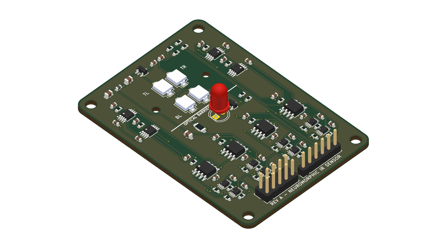 | 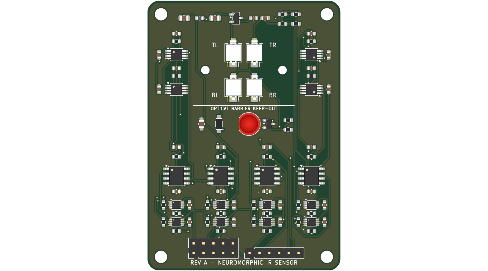 |
Each quadrant operates through an independent analog signal chain:
[Photodiode Pair (BPW34S)]
        │
        ▼
[Transimpedance Amplifier (TIA)]  ──> OPA381 Precision Stage (RF = 18.0k, CF = 47pF, VREF = 1.25V)
        │
        ▼
[High-Pass Differentiator (AC Coupling)] ──> Extracts Temporal Contrast (RA = 22.0k, CA = 100nF, tau = 2.2ms)
        │
        ├──> (+) Positive Threshold Comparator (TLV3202, VTH_ON = 1.29V) ──> ON Event
        └──> (-) Negative Threshold Comparator (TLV3202, VTH_OFF = 1.21V) ──> OFF Event
        │
        ▼
[Monostable Pulse Shaper (74LVC1G123)] ──> Generates Calibrated Digital Spikes (~100 µs)
        │
        ▼
[Digital SPIKE Interface] ──> 2x10 Pin Header (J_FPGA)| Parameter | Specification | Notes |
|---|---|---|
| Dimensions | 50.0 mm × 70.0 mm | Rectangular form factor, 4 × M3 mounting holes at corners (3.5 mm inset) |
| Layer Count | 2 Layers | Top (F.Cu), Bottom (B.Cu) |
| Copper Weight | 1 oz (35 µm) | Standard FR4 substrate, 1.6 mm thickness |
| Ground Pours | Dual solid flooded planes | Top and bottom ground planes interconnected with low-impedance stitching |
| Minimum Trace / Space | 0.20 mm / 0.20 mm | 100% compliant with standard JLCPCB / PCBWay manufacturing rules |
| Minimum Drill / Annular | 0.30 mm drill / 0.60 mm pad | Standard via size throughout |
| Silkscreen Finish | Cleaned Front Silkscreen | Small 0402/0603 passive and dense IC reference designators hidden on F.SilkS (preserved on F.Fab for assembly), zero silkscreen-to-pad clipping |
| Supply Voltage | +3.3 V DC | Sourced via pin 2 of J_FPGA |
| Power Consumption | < 120 mA (quiescent) | Ferrite-bead isolated analog rail (FB1) |
Direct connection to FPGA GPIO bank.
| Pin | Net Name | Type | Description |
|---|---|---|---|
| 1 | GND | Power | System Ground |
| 2 | 3V3 | Power | +3.3 V Main Power Input |
| 3 | SPIKE_ON_TL | Output | Quadrant TL Positive Contrast Event |
| 4 | SPIKE_OFF_TL | Output | Quadrant TL Negative Contrast Event |
| 5 | SPIKE_ON_TR | Output | Quadrant TR Positive Contrast Event |
| 6 | SPIKE_OFF_TR | Output | Quadrant TR Negative Contrast Event |
| 7 | SPIKE_ON_BL | Output | Quadrant BL Positive Contrast Event |
| 8 | SPIKE_OFF_BL | Output | Quadrant BL Negative Contrast Event |
| 9 | SPIKE_ON_BR | Output | Quadrant BR Positive Contrast Event |
| 10 | SPIKE_OFF_BR | Output | Quadrant BR Negative Contrast Event |
| 11 | GND | Power | Digital Return Ground |
| 12 | AER_REQ | Output | Asynchronous Address-Event Request Line |
| 13 | AER_ACK | Input | Asynchronous Address-Event Acknowledge |
| 14 | RST_N | Input | Active-Low Hardware Reset |
| 15 | ADDR_0 | Output | Quadrant Address Bit 0 |
| 16 | ADDR_1 | Output | Quadrant Address Bit 1 |
| 17 | POLARITY | Output | Spike Polarity Indicator (1 = ON, 0 = OFF) |
| 18 | CLK_SYNC | Input | Optional FPGA Synchronous Sampling Clock |
| 19 | GND | Power | System Ground |
| 20 | 3V3_AUX | Power | Optional Auxiliary 3.3V Monitoring Rail |
Convenient oscilloscope probe points for calibration and signal integrity checking.
| Pin | Net Name | Type | Description |
|---|---|---|---|
| 1 | GND | Ground | Probe Ground Reference |
| 2 | VREF | Analog | Precision Low-Noise Bias Reference (1.250 V, REF3312) |
| 3 | VPHOTO_TL | Analog | Transimpedance Output: TL Quadrant |
| 4 | VPHOTO_TR | Analog | Transimpedance Output: TR Quadrant |
| 5 | VPHOTO_BL | Analog | Transimpedance Output: BL Quadrant |
| 6 | VPHOTO_BR | Analog | Transimpedance Output: BR Quadrant |
The analog front-end (AFE) and asynchronous spike generation stages have undergone complete SPICE and physical state-space simulation.
Detailed Engineering Report: See
docs/SIMULATION_REPORT.mdfor complete analytical derivations, phase margin calculations, and drift immunity proofs.
| Full AFE Transient Response (NGSPICE 46) | AC Stability & Bode Response (NGSPICE 46) |
|---|---|
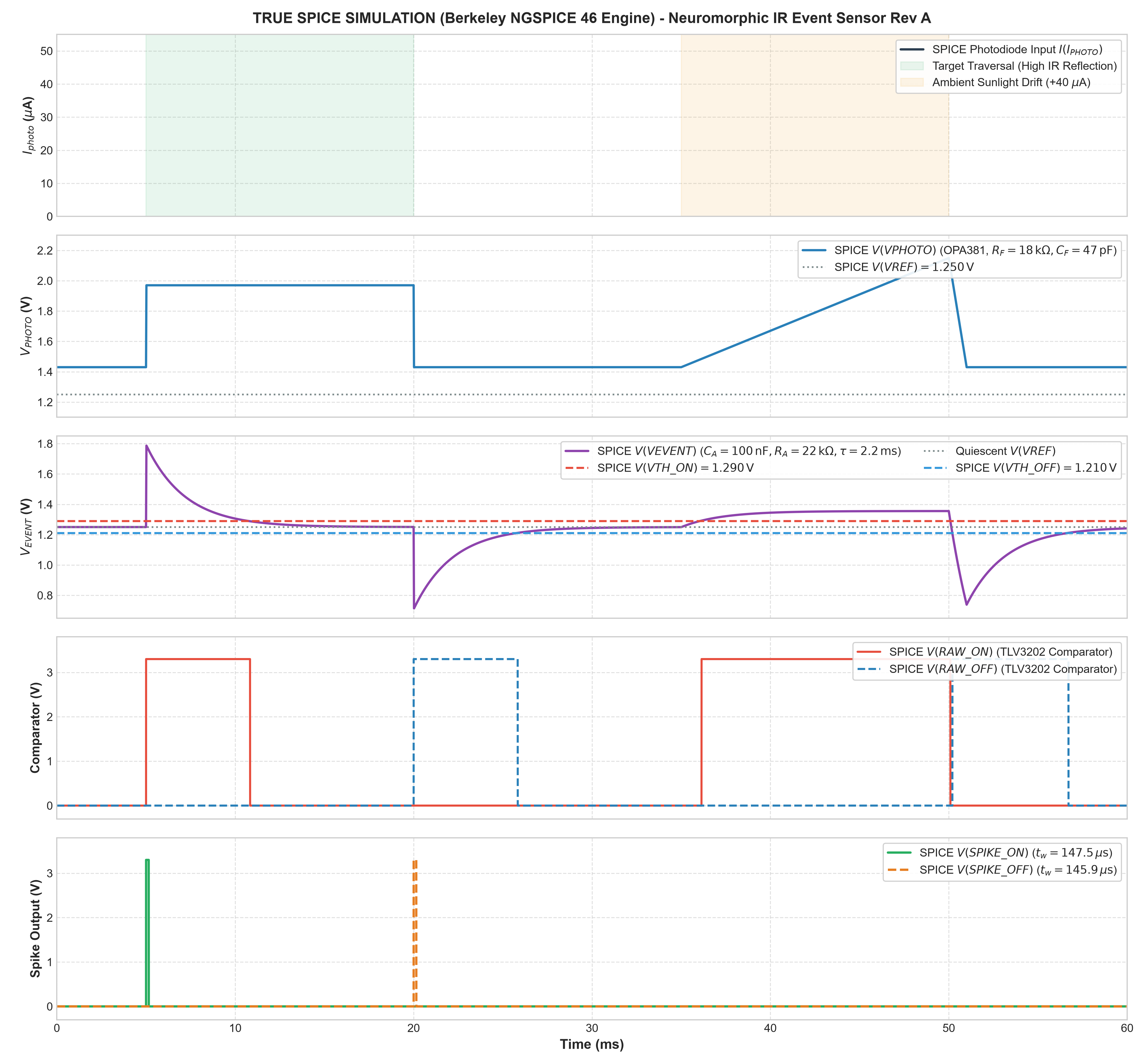 | 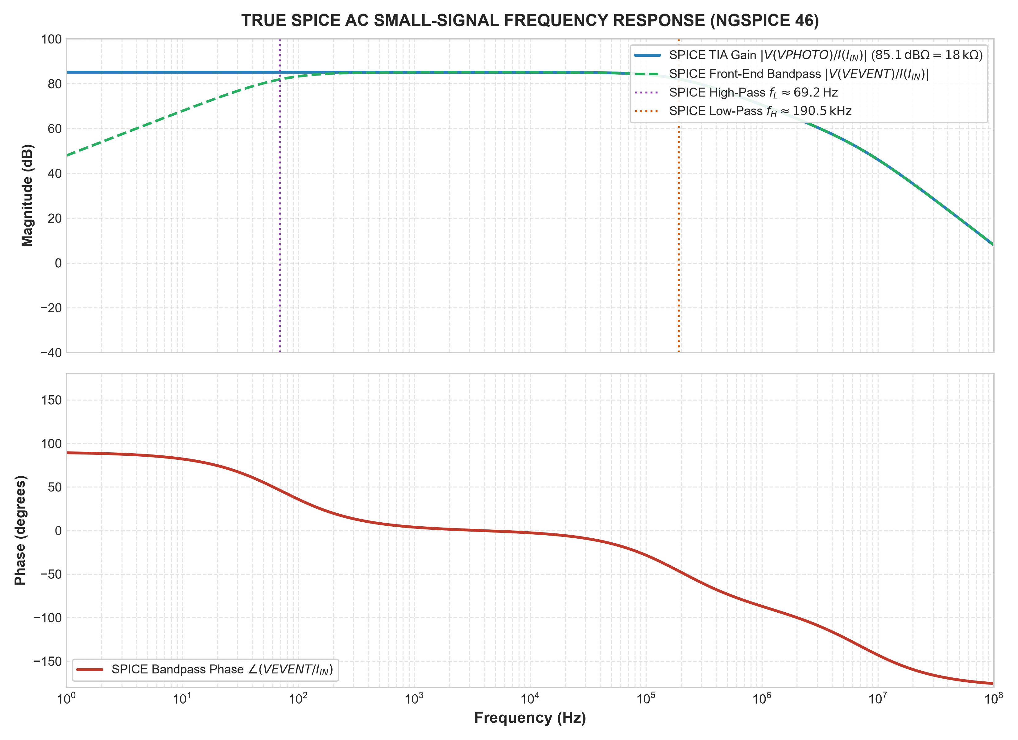 |
| Microsecond-Scale Spike Timing Detail (NGSPICE 46) |
|---|
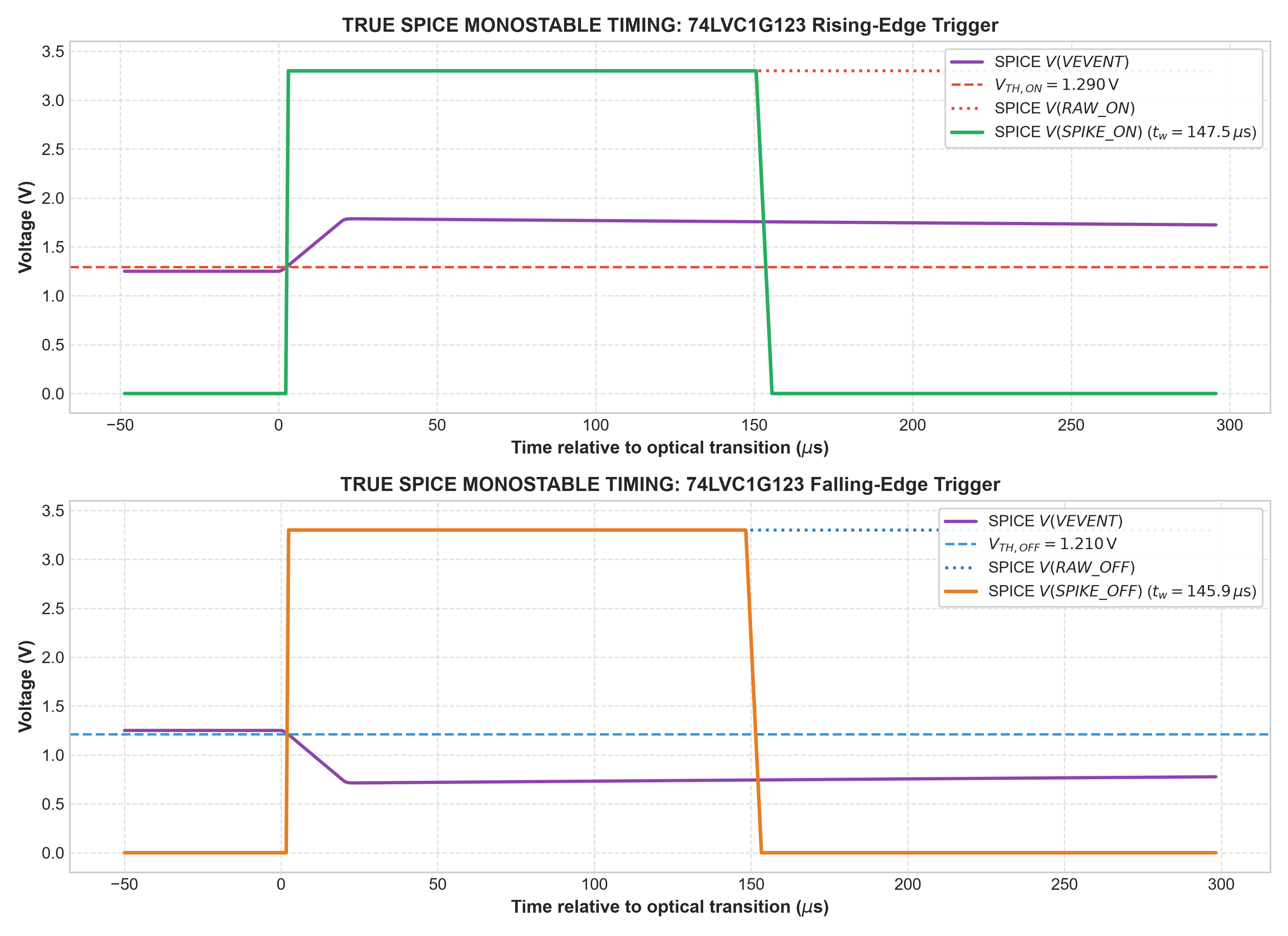 |
simulation/neuromorphic_afe.cir (native netlist executed via Berkeley NGSPICE 46 / PySpice)simulation/run_spice_simulation.py (python simulation/run_spice_simulation.py)simulation/simulate_afe.py (python simulation/simulate_afe.py)The board has been thoroughly verified using KiCad 10 CLI verification:
Ready-to-manufacture files are located in the production/ and gerbers/ directories:
production/neuromorphic-ir-event-sensor-revA.step (Ready for direct import into Onshape, SolidWorks, or FreeCAD for mechanical enclosure/lens housing modeling)production/neuromorphic-ir-event-sensor-revA-gerber.zipproduction/neuromorphic-ir-event-sensor-bom.csv (92 components, 27 unique groups)production/neuromorphic-ir-event-sensor-cpl.csvkicad-cli pcb drc --format json -o reports/drc_report.json neuromorphic-ir-event-sensor.kicad_pcbkicad-cli pcb export gerbers -o gerbers/ neuromorphic-ir-event-sensor.kicad_pcb
kicad-cli pcb export drill -o gerbers/ neuromorphic-ir-event-sensor.kicad_pcbpython simulation/run_spice_simulation.pypython simulation/simulate_afe.py| Qty | Value | Footprint | References |
|---|---|---|---|
| 21 | 100nF | Capacitor_SMD:C_0603_1608Metric | C10, C11, C12, C13, C14, C15, C16, C26, C30, C31, C32, C33, C34, C35, C36, C37 +5 |
| 8 | 12nF | Capacitor_SMD:C_0603_1608Metric | C17, C18, C19, C20, C21, C22, C23, C24 |
| 8 | 150R | Resistor_SMD:R_0603_1608Metric | R17, R18, R19, R20, R21, R22, R23, R24 |
| 8 | 2.0M | Resistor_SMD:R_0603_1608Metric | R32, R33, R34, R35, R36, R37, R38, R39 |
| 8 | 8.2k | Resistor_SMD:R_0603_1608Metric | R9, R10, R11, R12, R13, R14, R15, R16 |
| 8 | SN74LVC1G123DCU | Package_SO:VSSOP-8_2.3x2mm_P0.5mm | U9, U10, U11, U12, U13, U14, U15, U16 |
| 6 | 10.0k | Resistor_SMD:R_0603_1608Metric | R29, R30, R40, R41, R42, R43 |
| 4 | 18.0k | Resistor_SMD:R_0603_1608Metric | R1, R2, R3, R4 |
| 4 | 22k | Resistor_SMD:R_0603_1608Metric | R5, R6, R7, R8 |
| 4 | 47pF | Capacitor_SMD:C_0603_1608Metric | C1, C2, C3, C4 |
| 4 | MountingHole | MountingHole:MountingHole_3.2mm_M3 | H1, H2, H3, H4 |
| 4 | OPA381AIDGKR | Package_SO:MSOP-8_3x3mm_P0.65mm | U1, U2, U3, U4 |
| 4 | TLV3202AIDR | Package_SO:SOIC-8_3.9x4.9mm_P1.27mm | U5, U6, U7, U8 |
| 4 | VBPW34S | VBPW34S:XDCR_VBPW34S | D1, D2, D3, D4 |
| 3 | 10uF | Capacitor_SMD:C_0805_2012Metric | C27, C28, C29 |
| 2 | MountingHole | MountingHole:MountingHole_2.2mm_M2 | H5, H6 |
| 1 | 100R | Resistor_SMD:R_0603_1608Metric | R26 |
| 1 | 100k | Resistor_SMD:R_0603_1608Metric | R27 |
| 1 | 1uF | Capacitor_SMD:C_0603_1608Metric | C25 |
| 1 | 301k | Resistor_SMD:R_0603_1608Metric | R31 |
| 1 | 499k | Resistor_SMD:R_0603_1608Metric | R28 |
| 1 | 82R | Resistor_SMD:R_1206_3216Metric | R25 |
| 1 | AO3400A | Package_TO_SOT_SMD:SOT-23 | Q1 |
| 1 | Analog_Debug | Connector_PinHeader_2.54mm:PinHeader_1x06_P2.54mm_Vertical | J2 |
| 1 | BLM18AG601SN1D | Inductor_SMD:L_0603_1608Metric | FB1 |
| 1 | FPGA_Events_2x5 | Connector_PinHeader_2.54mm:PinHeader_2x05_P2.54mm_Vertical | J1 |
| 1 | LED_Enable_Input | Connector_PinHeader_2.54mm:PinHeader_1x02_P2.54mm_Vertical | J3 |
| 1 | RAW_OFF_BL | TestPoint:TestPoint_Pad_D1.0mm | TP8 |
| 1 | RAW_OFF_BR | TestPoint:TestPoint_Pad_D1.0mm | TP10 |
| 1 | RAW_OFF_TL | TestPoint:TestPoint_Pad_D1.0mm | TP4 |
| 1 | RAW_OFF_TR | TestPoint:TestPoint_Pad_D1.0mm | TP6 |
| 1 | RAW_ON_BL | TestPoint:TestPoint_Pad_D1.0mm | TP7 |
| 1 | RAW_ON_BR | TestPoint:TestPoint_Pad_D1.0mm | TP9 |
| 1 | RAW_ON_TL | TestPoint:TestPoint_Pad_D1.0mm | TP3 |
| 1 | RAW_ON_TR | TestPoint:TestPoint_Pad_D1.0mm | TP5 |
| 1 | REF3312AIDBZR | Package_TO_SOT_SMD:SOT-23-3 | U17 |
| 1 | TSAL6200 | LED_THT:LED_D5.0mm | D5 |
| 1 | VTH_OFF | TestPoint:TestPoint_Pad_D1.0mm | TP2 |
| 1 | VTH_ON | TestPoint:TestPoint_Pad_D1.0mm | TP1 |
strangeparts/niubi-headphones
Flexible circuit board design for adding a headphone jack to an iPhone 7

ldcyes/OpenDuck
已完成可编辑原理图、真实四层 PCB 和本地库。阶梯板面积 4510 mm²,比原 65×60 + 32×30 mm 两板总面积 4860 mm² 少 350 mm²(7.20%)。原 TDK 模块本体、四个安装孔和原 TDK 器件位置保留,回生电容采用原料号卧装,J1 因实际拔插通道冲突改为同系列 BM08 顶插。当前为工程候选,未制造,未完成热、回生瞬态、低电量或行走验收。

RobieElliz/esp32InductanceMeterV2
Portable ESP32 Inductance Meter: A low-cost, high-precision tool with dual 100nF/5µF refs, a TLV3202 comparator, fast USB-C (IP2312) charging, and a 2.4-inch OLED display for real-time readings.


open3doled/open-3d-oled
If running windows 11 or 10 with DPI scaling be sure to disable it as follows. 1) Right click properties on 3dplayer.exe in the 3DPlayer folder 2) Click on "Compatability" tab then click on the button at the bottom…

RyanHailey21/neuromorphic-IR-hand-assembled
All through-hole re-implementation of the Rev A neuromorphic IR event sensor: no SMD parts, solderable with a basic iron.

frameprobe/frameprobe
End-to-end display latency measurement: the time from a mouse click to a visible change on screen, measured with a photodiode strapped to the monitor.

It measures 50 × 70 mm and has 2 copper layers, 1.6 mm thick.
123 parts, built around the SN74LVC1G123DCU, TLV3202AIDR(LX), REF3312AIDBZR and VBPW34S. The full list of its parts is on this page, with links to each part's symbol and footprint where PCBKit's library has them.
From the RyanHailey21/neuromorphic-ir-event-sensor repository on GitHub, at the commit this page was made from: the board is neuromorphic-ir-event-sensor.kicad_pcb and its schematic headless_candidate/neuromorphic-ir-event-sensor.kicad_sch. PCBKit opens the board in the browser, with nothing to install.
Its repository states no licence, so its author keeps all rights: ask RyanHailey21 before reusing the design.