Skip to the content
4 layers28 × 28 mmKestrel gps, the printed circuit board in 3D

Kestrel GPS: u-blox MAX-M10S under a 25 mm ceramic patch with an LIS3MDL compass, for Betaflight, INAV and ArduPilot. 28 x 28 mm 4-layer KiCad 10 board, DRC clean, with gerbers, BOM, CPL and STEP.

Size
28 × 28 mm
Copper layers
4
Thickness
1.6 mm
Parts
14
Nets
21
Pads
59
Tracks, vias
116, 54
Pours
5
Routed
Yes
KiCad
KiCad 10.0 (file 20260206)
Created
6 Oct 2026
Updated
6 Oct 2026

Overview

Kestrel gps is an open-source printed circuit board by HeyPCB, from the HeyPCB/kestrel-gps repository on GitHub, published under the CERN-OHL-S-2.0 licence. It is a 4-layer board of 28 × 28 mm with 14 parts on 21 nets, routed with 116 tracks and 54 vias.

It is built around the MAX-M10S-00B, LIS3MDL and XC6206P332MR-G, with the CL21A106KAYNNNE and SM06B-SRSS-TB(LF)(SN) among its other parts. Its parts include 8 capacitors, 3 ICs and 1 connector. It belongs with the radio and wireless and robots and motor control boards of this library.

Main components

5

README

README.md

Kestrel GPS: GNSS and compass module

A u-blox MAX-M10S under a 25 mm ceramic patch, with an LIS3MDL compass, on a 28 x 28 mm board that plugs 1:1 into the Kestrel H7.
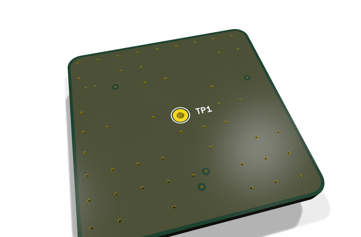
Kestrel GPS, raytraced in KiCad

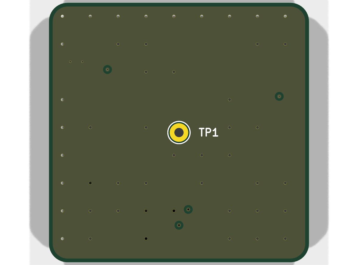
The Kestrel GPS is the navigation module of Kestrel. Its top face is unbroken ground for the patch antenna, whose feed pin passes through a plated hole to one 2.5 mm track to the receiver; every part is on the bottom face. Betaflight, INAV and ArduPilot all have drivers for both chips.

LayersSizeFootprints (LCSC parts)NetsConnections routedRouted viasERC errors / warningsDRC errors / warnings / unconnected / parityParts per board, 10-board build
428 x 28 mm14 (12)1038 -> 0 open60 / 10 / 0 / 0 / 0$15.31

Not fabricated, assembled, powered or flown yet. Every number on this page is measured by KiCad 10.0.6 on the files in this repository (report.json, fab/erc.json, fab/drc.json) or read from the live JLC/LCSC catalogue (bom_cost.md: parts only, at a 10-board build's price tier with JLC's Extended-part fee; the bare PCB and assembly are quoted at order time). The 1 ERC warning is KiCad's pin-type check on a pin the design ties to a rail on purpose: the LIS3MDL's SA1 tied to Vdd_IO selects I2C address 0x1E.

The whole drone: spec, build guide, BOM, measured resultsHeyPCB/kestrel
KiCad 10 projectkicad/
Gerbers, drill, BOM, CPL, STEP, schematic PDFfab/
Firmwarenone to build: the flight controller's firmware drives the MAX-M10S and the LIS3MDL
Rendersfront, back, hero, Circuit World thumbnail
Brief and generatordesign/

front back

What's on it

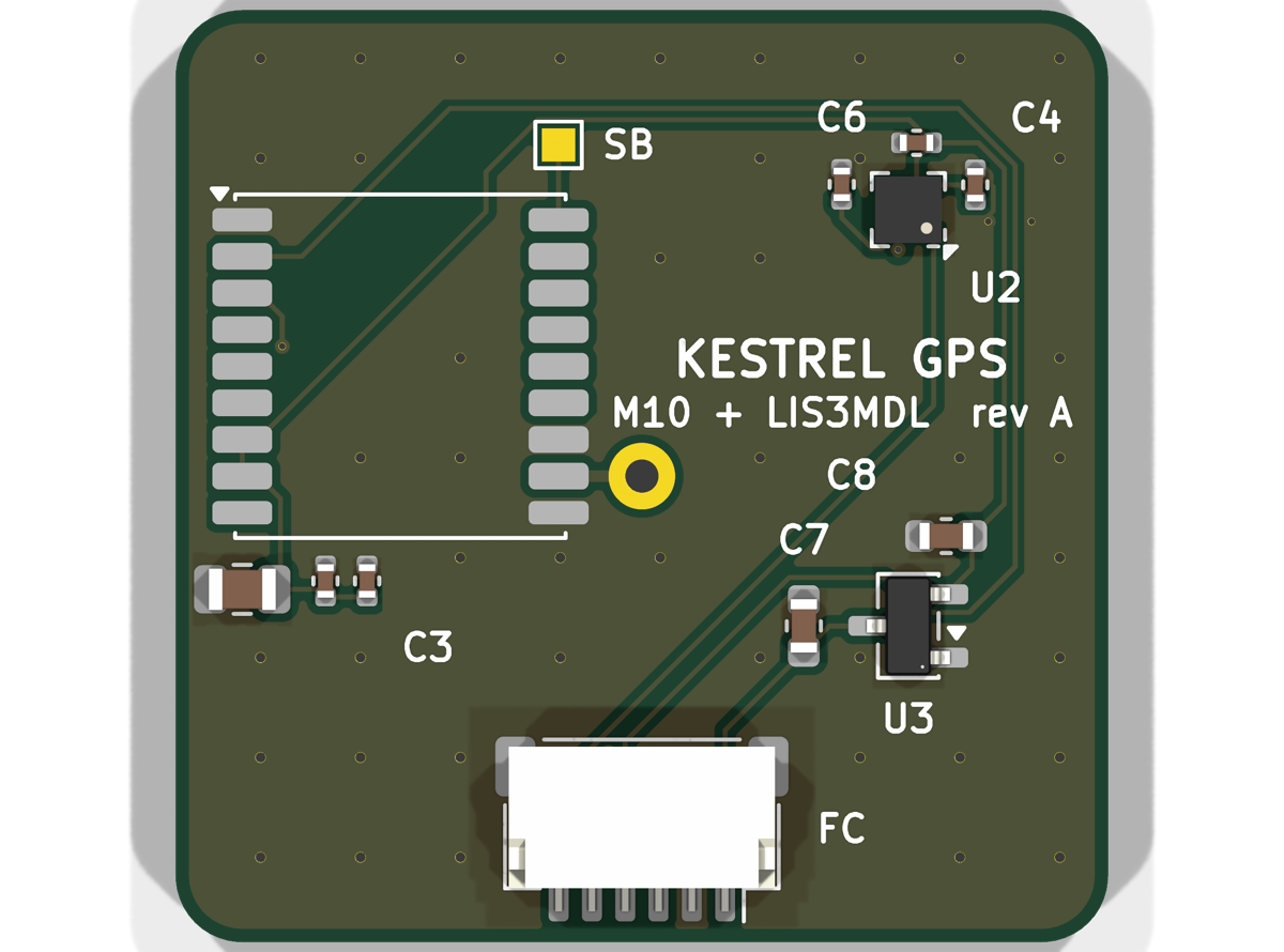
  • Receiver: u-blox MAX-M10S: GPS, Galileo, BeiDou and GLONASS at once, with an integrated LNA and SAW filter.
  • Antenna: a 25 x 25 mm passive ceramic patch (bought separately) on the top face's ground, its feed pin in a 1.0 mm plated hole.
  • Compass: ST LIS3MDL on I2C at 0x1E, in the corner farthest from the receiver.
  • Power: XC6206 3.3 V LDO from the port's 5 V.
  • Connector: JST-SH 6, 1:1 with the Kestrel H7's GPS port.
  • Cold start at every power-up (23-28 s by the data sheet): V_BCKP is left open because JLC stocks no backup cell with a KiCad footprint.

Ordering

4 layers, 1.6 mm, 1 oz copper; parts on the bottom face only (the top is the antenna's ground). Upload fab/kestrel_gps_gerbers.zip, fab/kestrel_gps_bom.csv and fab/kestrel_gps_cpl_jlc.csv to JLCPCB: every part has an LCSC number. Bring-up, one board at a time, is in the hub's BUILD.md.

How it was made

Designed with the HeyPCB method on KiCad 10.0.6, headless, by the heypcb-kicad pipeline: a written brief composed from reusable circuit blocks, every pin from KiCad's own symbol library, every part bound to an LCSC number from a dated catalogue read, then ERC, a netlist round trip, locked placement, Freerouting 2.4.1, pours and stitching, silkscreen, DRC with schematic parity, DFM and a fab gate, each stage gated by a measurement. design/make_brief.py regenerates the brief (outline, part locks, net classes) from code.

Part of Kestrel, a 5-inch 6S FPV quad's electronics.

License

Hardware: CERN-OHL-S v2. KiCad's symbol, footprint and 3D libraries used in the design are CC-BY-SA 4.0 with the KiCad library exception.

Parts

14
QtyValueFootprintReferences
4100nFCapacitor_SMD:C_0402_1005MetricC2, C3, C4, C5
21uFCapacitor_SMD:C_0603_1608MetricC7, C8
110uFCapacitor_SMD:C_0805_2012MetricC1
11uFCapacitor_SMD:C_0402_1005MetricC6
1ANTTestPoint:TestPoint_THTPad_D2.0mm_Drill1.0mmTP1
1GPSConnector_JST:JST_SH_SM06B-SRSS-TB_1x06-1MP_P1.00mm_HorizontalJ1
1LIS3MDLPackage_LGA:LGA-12_2x2mm_P0.5mmU2
1MAX-M10SRF_GPS:ublox_MAXU1
1SAFEBOOTTestPoint:TestPoint_Pad_1.0x1.0mmTP2
1XC6206P332MRPackage_TO_SOT_SMD:SOT-23-3U3

Similar boards

  • 4 layers46 × 46 mmPlacement, the printed circuit board in 3D

    Placement

    anil08607/stm32-smartwatch

    A 46 × 46 mm, four-layer Bluetooth smartwatch PCB with a Nordic nRF52810-QFAA, 240 × 240 SPI LCD interface, BMA456 accelerometer, battery-backed PCF8563 RTC, USB-C 5 V charging, protected single-cell battery interface…

    71 parts
  • 2 layers53.9 × 62.6 mmMoon light, the printed circuit board in 3D

    Moon light

    HeyPCB/moon-light

    Luna, the night-light moon: A sleepy moon that turns on at dusk and tucks itself in after you fall asleep. KiCad 10, heypcb.ai merch.

    36 parts1CERN-OHL-S-2.0
  • 4 layers101 × 51.5 mmQuack core, the printed circuit board in 3D

    Quack core

    HeyPCB/quack-core

    Brain board for the Open Duck Mini: Pi Zero 2W carrier, 14-servo STS bus, fused 2S power path in stitched copper zones (15-18 A battery side), USB-C charging with balancing, IMU.

    138 parts1CERN-OHL-S-2.0
  • 4 layers128 × 51.4 mmQuack face, the printed circuit board in 3D

    Quack face

    HeyPCB/quack-face

    Face board for the Open Duck Mini's head: eye LEDs, projector driver, I2S amp and mic, antenna servos, shaped to the head. 4-layer KiCad 10 board plus printed standoffs, fit-checked in the head CAD.

    55 partsCERN-OHL-S-2.0
  • 4 layers64.6 × 55.2 mmWhisker, the printed circuit board in 3D

    Whisker

    HeyPCB/whisker

    Drop-in controller for Petoi's Nybble robot cat running the stock OpenCat firmware: ATmega328P, PCA9685, MPU-6050, USB-C, 3 A buck, protected battery input. 4-layer KiCad 10 board plus printed cradle.

    118 partsCERN-OHL-S-2.0
  • 2 layers44 × 72 mmConsole, the printed circuit board in 3D

    Console

    mrkct/console

    47 parts
  • 4 layers87 × 107.4 mmSl v4, the printed circuit board in 3D

    Sl v4

    jackw01/scanlight

    A better light source for scanning color negative film

    154 parts397CERN-OHL-W-2.0
  • 2 layers95 × 24.7 mmJs320-faceplate, the printed circuit board in 3D

    Js320-faceplate

    tag-designs/hardware

    Hardware designs for tags and bases

    20 parts2CERN-OHL-P-2.0

Questions

How big is the Kestrel gps PCB?

It measures 28 × 28 mm and has 4 copper layers, 1.6 mm thick.

What parts does the Kestrel gps use?

14 parts, built around the MAX-M10S-00B, LIS3MDL, XC6206P332MR-G and CL21A106KAYNNNE. The full list of its parts is on this page, with links to each part's symbol and footprint where PCBKit's library has them.

Where can I download the Kestrel gps KiCad files?

From the HeyPCB/kestrel-gps repository on GitHub, at the commit this page was made from: the board is kicad/kestrel_gps.kicad_pcb and its schematic kicad/kestrel_gps.kicad_sch. PCBKit opens the board in the browser, with nothing to install.

Can I use the Kestrel gps design in my own project?

Its repository publishes it under the CERN-OHL-S-2.0 licence: you may reuse it on that licence's terms (keep the author's notice, and for a copyleft licence share your changes alike).