8 layers50 × 50 mm

 HexFud/OptiLogic-16-Pro
A logic analyzer with 16 channels that can also watch two fiber network links at the same time
OptiLogic-16-Pro is an open-source printed circuit board by HexFud, from the HexFud/OptiLogic-16-Pro repository on GitHub. It is an 8-layer board of 230 × 145.3 mm with 342 parts on 679 nets, routed with 5,536 tracks and 1,084 vias.
It is built around the KSZ9031RNXCA, FT601Q-B-T and W25Q128JVSIQ, with the LMH7324SQ, MT41K256M16HA-CN and TLV75512PDBV among its other parts. Its parts include 144 resistors, 124 capacitors, 25 ICs, 19 diodes and 9 connectors. It belongs with the sensors and measurement boards of this library.


OptiLogic-16 Pro is a custom built, FPGA-based 16-channel logic analyzer and network monitor designed from scratch from PCB design and component selection to firmware development and 3D modeling. Featuring a Xilinx Kintex-7 FPGA 500 MSa/s sampling programmable input thresholds 4 Gbit DDR3 memory three SFP ports Gigabit Ethernet and USB 3.0, it is designed for high-speed digital signal analysis, hardware debugging, and network data acquisition.
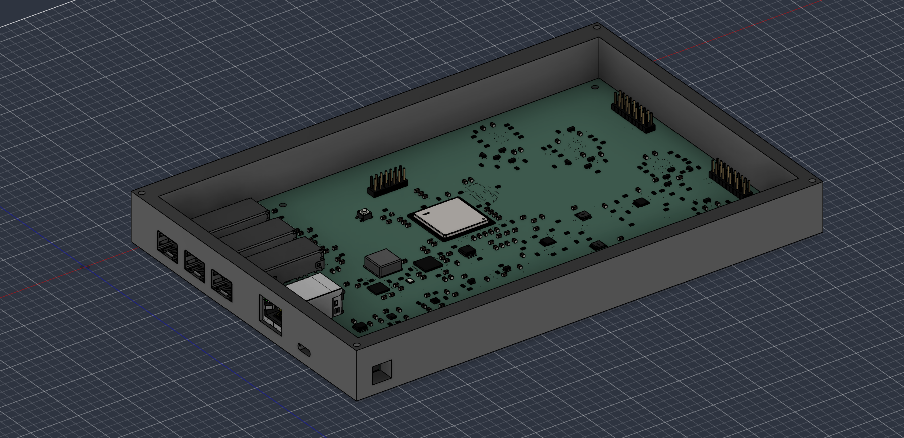
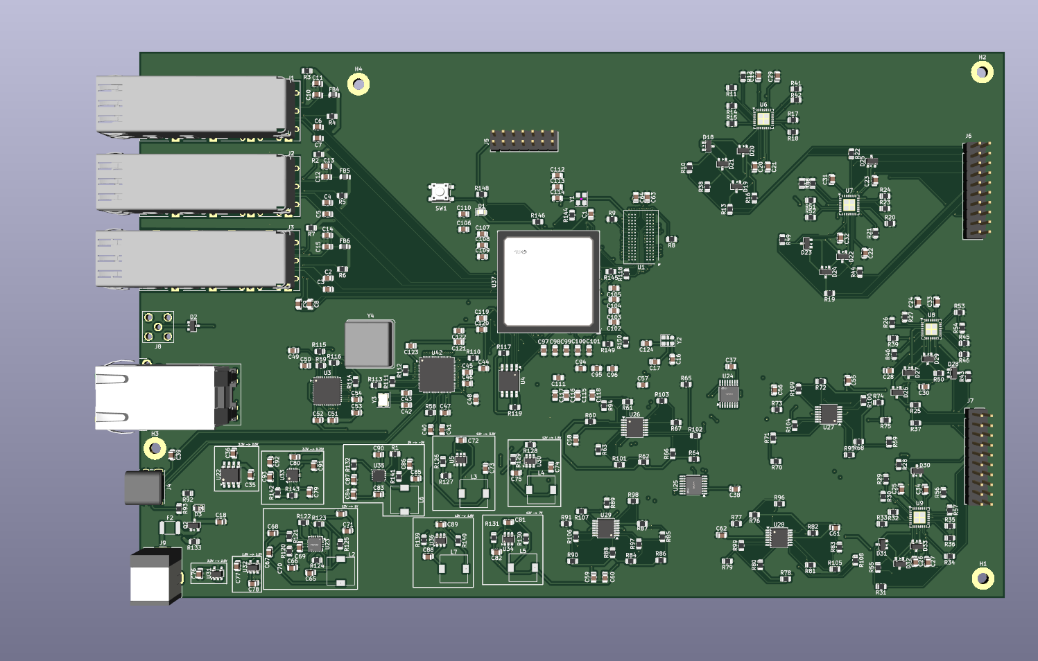
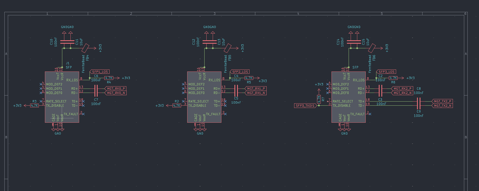
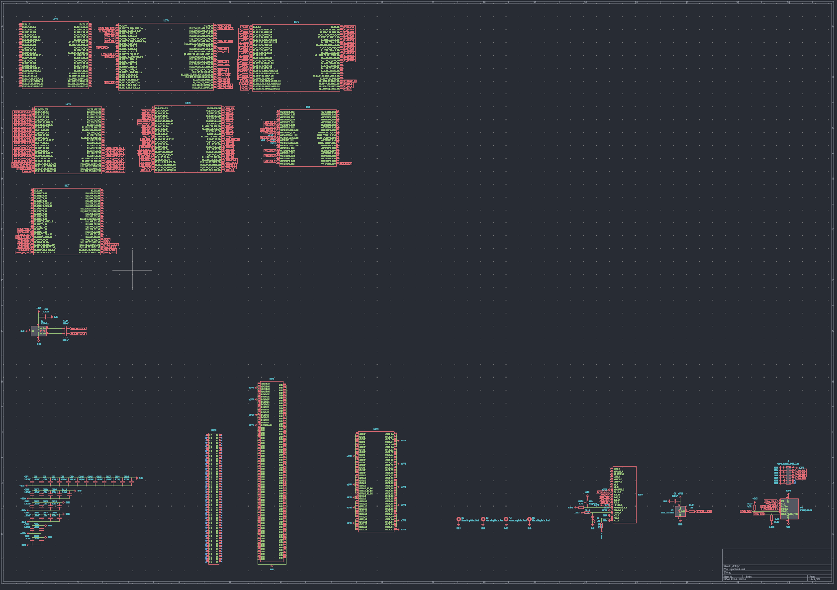
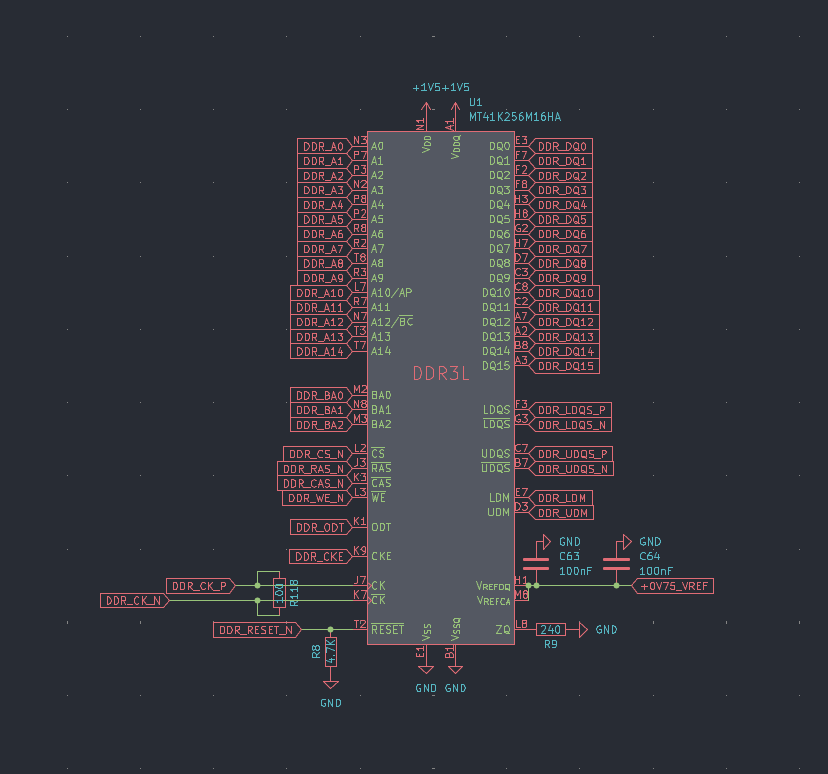
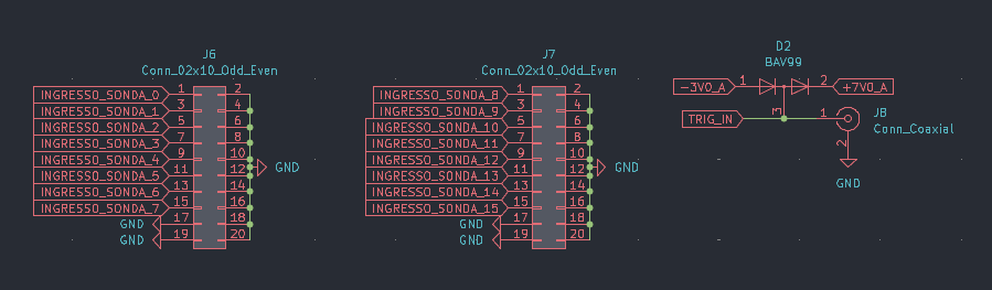
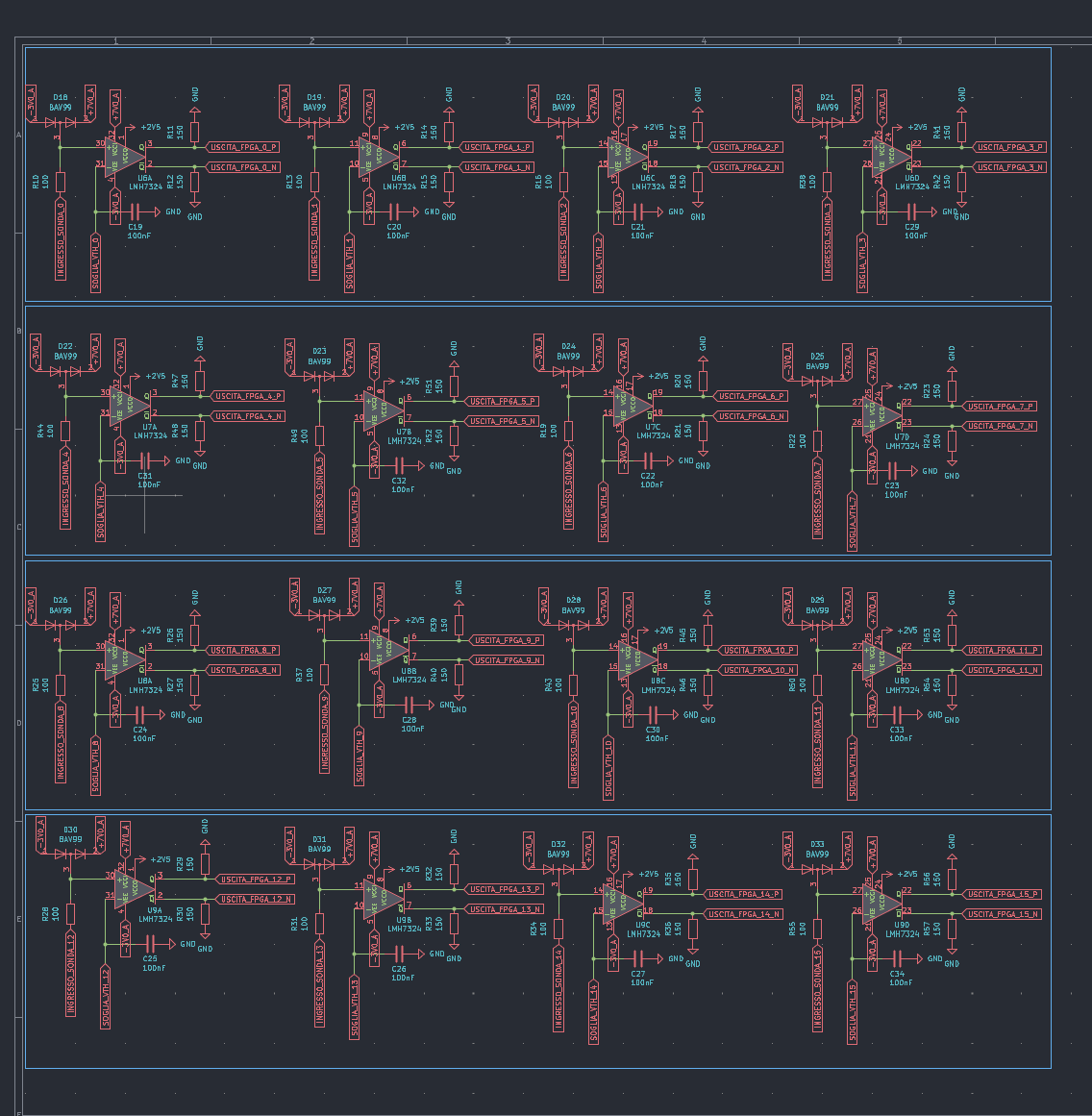
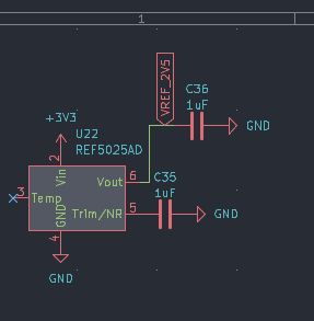
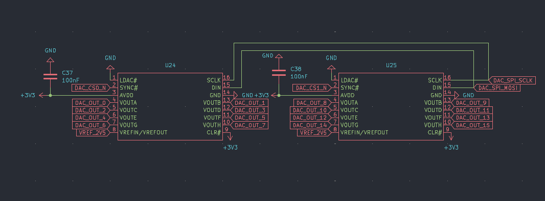
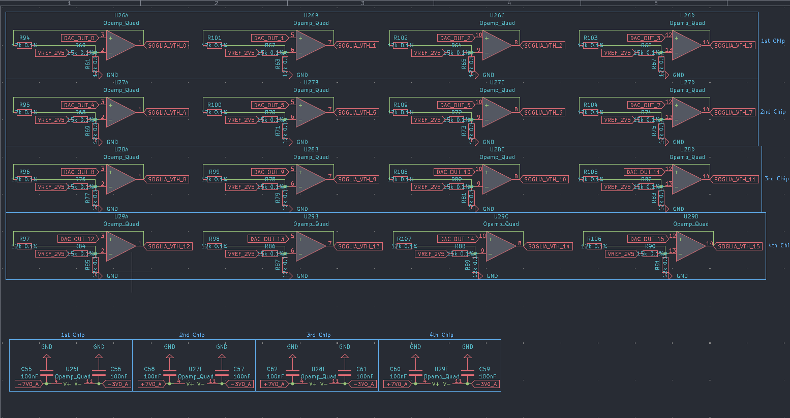
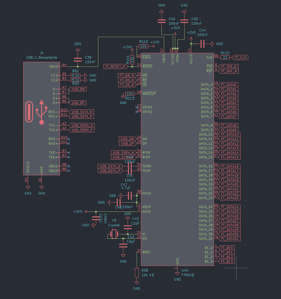
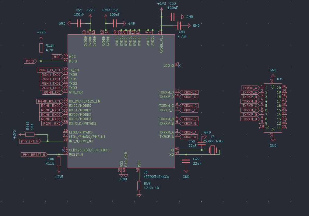
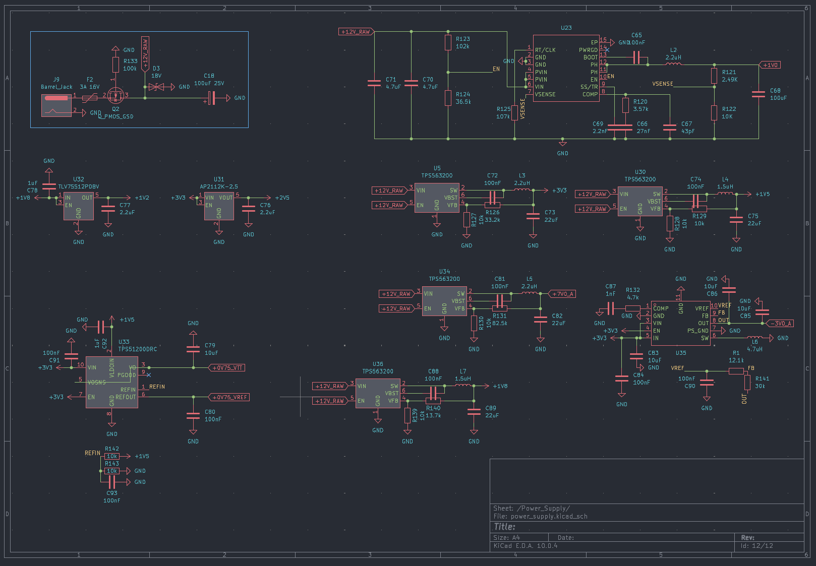
I designed an 8-layer PCB that has 16 digital inputs united by 4 comparators. The board runs with 12V DC current with a standard barrel jack connector:
The PCB has a precise layer structure:
To make sure the logic analyzer can sample at 500 MSa/s without struggling with signal integrity, I had to select specialized components:
VCCO) at +2.5V, the RSPECL outputs naturally shift to LVDS levels, allowing direct connection to the FPGA without complex external resistor networks.My project doesn't have a built-in USB-to-JTAG programmer. To flash the firmware you need a Xilinx Platform Cable USB or a JTAG adapter wired to the connector. You must use the AMD/Xilinx Vivado Design Suite to upload the firmware into the QSPI Flash.
In AMD/Xilinx Vivado (Compilation):
XC7K70T-2FBG676I.write_cfgmem -format bin -interface spix4 -size 16 -loadbit "up 0x0 ./project_name.runs/impl_1/optilogic_16_pro_top.bit" -file ./optilogic_16_pro_flash.binIn Vivado Hardware Manager (Flashing):
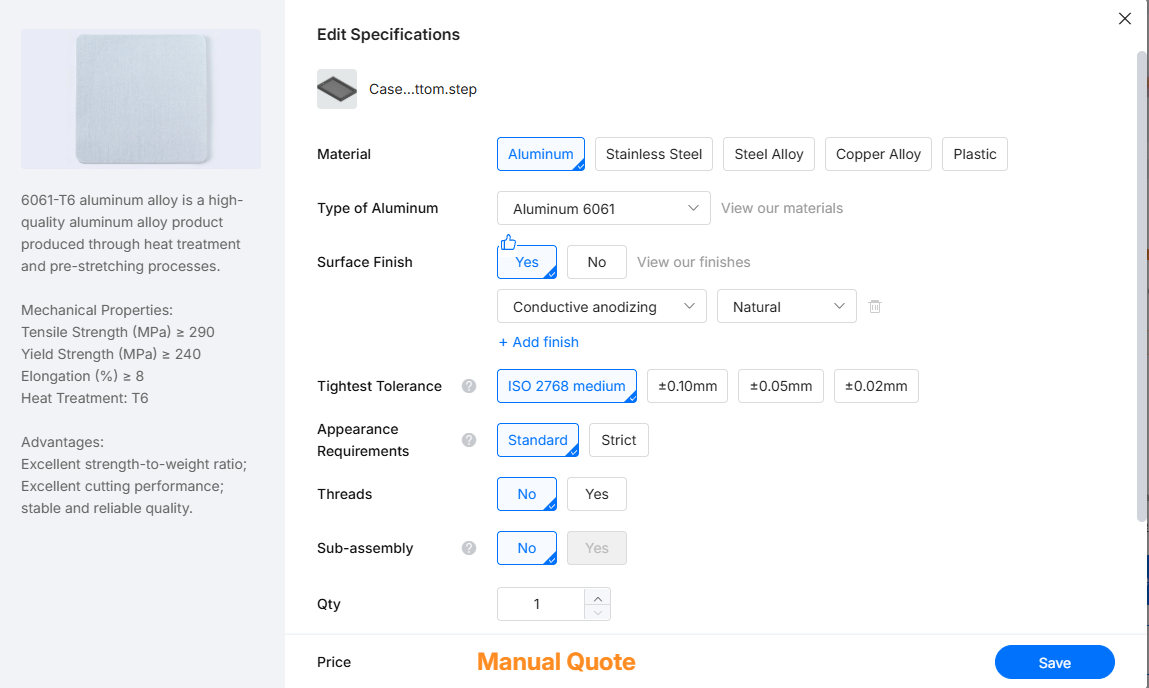
xc7k70t_0 device and select "Add Configuration Memory Device".w25q128-spi-x1_x2_x4 part and select it..bin file ensure "Erase, Program, Verify" is selected, and click "Start Programming". If everything goes right you'll see a success message. Power-cycle the board to boot the firmware.The Kintex-7 FPGA, FT601Q bridge, KSZ9031 PHY, and switching regulators generate a lot of heat (50°C–60°C) during continuous sampling. The LMH7324 comparators also dissipate heat into the PCB internal GND plane. To dissipate the thermal load and shield the board from radio frequency interference the board must be enclosed in a CNC-machined aluminum case.
I suggest using these settings on JLCPCB before putting it into production
This project includes experimental software and hardware designs. Assembly documentation and firmware are still under development and may contain bugs, errors, or incomplete features. By using, building, or modifying this project, you acknowledge that:
By proceeding, you accept all risks and agree to these conditions. If you do not acknowledge these risks and conditions, please do not use or build this project.
| Qty | Value | Footprint | References |
|---|---|---|---|
| 90 | 100nF | Capacitor_SMD:C_0805_2012Metric | C1, C10, C100, C101, C102, C103, C106, C107, C108, C109, C111, C112, C113, C114, C115, C116 +74 |
| 32 | 12k 0.1% | Resistor_SMD:R_0805_2012Metric | R61, R63, R65, R67, R69, R71, R100, R101, R102, R103, R104, R105, R106, R107, R108, R109 +16 |
| 32 | 150 | Resistor_SMD:R_0805_2012Metric | R11, R12, R14, R15, R17, R18, R20, R21, R23, R24, R26, R27, R29, R30, R32, R33 +16 |
| 18 | 100 | Resistor_SMD:R_0805_2012Metric | R10, R13, R16, R19, R22, R25, R28, R31, R34, R37, R38, R43, R44, R49, R118, R145 +2 |
| 17 | BAV99 | Package_TO_SOT_SMD:SOT-23 | D2, D18, D19, D20, D21, D22, D23, D24, D25, D26, D27, D28, D29, D30, D31, D32 +1 |
| 16 | 15k 0.1% | Resistor_SMD:R_0805_2012Metric | R60, R62, R64, R66, R68, R70, R72, R74, R76, R78, R80, R82, R84, R86, R88, R90 |
| 10 | 10k | Resistor_SMD:R_0805_2012Metric | R111, R112, R113, R127, R128, R129, R130, R139, R142, R143 |
| 8 | 4.7K | Resistor_SMD:R_0805_2012Metric | R2, R3, R4, R5, R6, R7, R8, R114 |
| 7 | 10uF | Capacitor_SMD:C_0805_2012Metric | C11, C13, C15, C79, C83, C85, C86 |
| 7 | 4.7k | Resistor_SMD:R_0805_2012Metric | R117, R119, R132, R146, R148, R149, R150 |
| 7 | 4.7uF | Capacitor_SMD:C_0805_2012Metric | C47, C54, C70, C71, C104, C105, C110 |
| 4 | 1uF | Capacitor_SMD:C_0805_2012Metric | C35, C36, C78, C92 |
| 4 | 22uF | Capacitor_SMD:C_0805_2012Metric | C73, C75, C82, C89 |
| 4 | LMH7324 | Package_DFN_QFN:WQFN-32-1EP_5x5mm_P0.5mm_EP3.1x3.1mm | U6, U7, U8, U9 |
| 4 | MountingHole_Pad | MountingHole:MountingHole_3mm_Pad | H1, H2, H3, H4 |
| 4 | Opamp_Quad | Package_SO:TSSOP-14_4.4x5mm_P0.65mm | U26, U27, U28, U29 |
| 4 | TPS563200 | Package_TO_SOT_SMD:SOT-23-6 | U5, U30, U34, U36 |
| 3 | 10K | Resistor_SMD:R_0805_2012Metric | R115, R116, R122 |
| 3 | 2.2uH | Inductor_SMD:L_7.3x7.3_H3.5 | L2, L3, L5 |
| 3 | FerriteBead | Inductor_SMD:L_0805_2012Metric | FB4, FB5, FB6 |
| 3 | SFP | Connector:Connector_SFP_and_Cage | J1, J2, J3 |
| 2 | 1.5uH | Inductor_SMD:L_7.3x7.3_H3.5 | L4, L7 |
| 2 | 12pF | Capacitor_SMD:C_0805_2012Metric | C42, C43 |
| 2 | 2.2uF | Capacitor_SMD:C_0805_2012Metric | C76, C77 |
| 2 | 22pF | Capacitor_SMD:C_0805_2012Metric | C49, C50 |
| 2 | 5.1k | Resistor_SMD:R_0805_2012Metric | R92, R93 |
| 2 | Conn_02x10_Odd_Even | Connector_PinHeader_2.54mm:PinHeader_2x10_P2.54mm_Vertical | J6, J7 |
| 2 | ~ | EasyEDA_Lib:TSSOP-16_L5.0-W4.4-P0.65-LS6.4-BL | U24, U25 |
| 1 | 100k | Resistor_SMD:R_0805_2012Metric | R133 |
| 1 | 100uF | Capacitor_SMD:C_0805_2012Metric | C68 |
| 1 | 100uF 25V | Capacitor_SMD:C_0805_2012Metric | C18 |
| 1 | 102k | Resistor_SMD:R_0805_2012Metric | R123 |
| 1 | 107k | Resistor_SMD:R_0805_2012Metric | R125 |
| 1 | 12.1k | Resistor_SMD:R_0805_2012Metric | R1 |
| 1 | 12.1k 1% | Resistor_SMD:R_0805_2012Metric | R59 |
| 1 | 125MHz | Oscillator:Oscillator_SMD_SiTime_PQFD-6L_3.2x2.5mm | Y2 |
| 1 | 12k 1% | Resistor_SMD:R_0805_2012Metric | R58 |
| 1 | 13.7k | Resistor_SMD:R_0805_2012Metric | R140 |
| 1 | 18V | Diode_SMD:D_0805_2012Metric | D3 |
| 1 | 1nF | Capacitor_SMD:C_0805_2012Metric | C87 |
| 1 | 2.2nF | Capacitor_SMD:C_0805_2012Metric | C69 |
| 1 | 2.49K | Resistor_SMD:R_0805_2012Metric | R121 |
| 1 | 22 | Resistor_SMD:R_0805_2012Metric | R110 |
| 1 | 240 | Resistor_SMD:R_0805_2012Metric | R9 |
| 1 | 25.000 MHz | Oscillator:Oscillator_DIP-8 | Y4 |
| 1 | 27nF | Capacitor_SMD:C_0805_2012Metric | C66 |
| 1 | 3.57k | Resistor_SMD:R_0805_2012Metric | R120 |
| 1 | 30k | Resistor_SMD:R_0805_2012Metric | R141 |
| 1 | 33 | Resistor_SMD:R_0805_2012Metric | R144 |
| 1 | 33.2k | Resistor_SMD:R_0805_2012Metric | R126 |
| 1 | 36.5k | Resistor_SMD:R_0805_2012Metric | R124 |
| 1 | 3A 16V | Fuse:Fuse_1812_4532Metric | F2 |
| 1 | 4.7uH | Inductor_SMD:L_7.3x7.3_H3.5 | L6 |
| 1 | 43pF | Capacitor_SMD:C_0805_2012Metric | C67 |
| 1 | 82.5k | Resistor_SMD:R_0805_2012Metric | R131 |
| 1 | ACO-xxxMHz | Oscillator:Oscillator_SMD_Abracon_ASE-4Pin_3.2x2.5mm | Y1 |
| 1 | AP2112K-2.5 | Package_TO_SOT_SMD:SOT-23-5 | U31 |
| 1 | Barrel_Jack | Connector_BarrelJack:BarrelJack_CUI_PJ-063AH_Horizontal | J9 |
| 1 | Conn_02x07_Odd_Even | Connector_PinHeader_2.54mm:PinHeader_2x07_P2.54mm_Vertical | J5 |
| 1 | Conn_Coaxial | Connector_Coaxial:SMA_Amphenol_132203-12_Horizontal | J8 |
| 1 | Crystal | Crystal:Crystal_SMD_3225-4Pin_3.2x2.5mm | Y3 |
| 1 | FT601Q | Package_DFN_QFN:QFN-76-1EP_9x9mm_P0.4mm_EP5.81x6.31mm | U42 |
| 1 | KSZ9031RNXCA | Package_DFN_QFN:QFN-48-1EP_7x7mm_P0.5mm_EP5.15x5.15mm | U3 |
| 1 | LED | LED_SMD:LED_0805_2012Metric | D1 |
| 1 | MT41K256M16HA | Package_BGA:Micron_FBGA-96_9x14mm_Layout9x16_P0.8mm | U1 |
| 1 | Q_PMOS_GSD | Package_TO_SOT_SMD:SOT-23 | Q2 |
| 1 | REF5025AD | Package_SO:SOIC-8_3.9x4.9mm_P1.27mm | U22 |
| 1 | SW_Push | Button_Switch_SMD:SW_SPST_PTS647_Sx38 | SW1 |
| 1 | TLV75512PDBV | Package_TO_SOT_SMD:SOT-23-5 | U32 |
| 1 | TPS51200DRC | Package_SON:VSON-10-1EP_3x3mm_P0.5mm_EP1.65x2.4mm | U33 |
| 1 | USB_C_Receptacle | Connector_USB:USB_C_Receptacle_GCT_USB4085 | J4 |
| 1 | W25Q128JVS | Package_SO:SOIC-8_5.3x5.3mm_P1.27mm | U4 |
| 1 | ~ | EasyEDA_Lib:VSON-10_L3.0-W3.0-P0.50-TL-EP-1 | U35 |
| 1 | ~ | EasyEDA_Lib:VQFN-14_L3.5-W3.5-P0.50-BL-EP_TPS54622RHLT | U23 |
| 1 | ~ | EasyEDA_Lib:FBGA-676_L27.0-W27.0-R26-C26-P1.00-BL | U37 |
| 1 | ~ | EasyEDA_Lib:RJ45-TH_0826-1X1T-HT-F | RJ1 |


kitspace-forks/reform-kintex-som
This is the open hardware system-on-module featuring the Xilinx/AMD Kintex-7 FPGA (XC7K160T or XC7K325T) and 2GB DDR3 RAM.


embeddedos-org/eCAD-Hardware-Products
Hardware designs + EE docs + Board datasheets of Multiple products

cfbird/usb3-sdr
USB3 direct-sampling HF SDR: AD9649 ADC -> ECP5 FPGA DDC -> FT601 USB 3. KiCad 9 + Verilog, co-designed by Claude and Gemini (AGY).

jayis1/hacker-devices
Full-cycle hardware designs for security research devices — each device is a subfolder with its own README, schematics, PCB layout, and software stack
It measures 230 × 145.3 mm and has 8 copper layers, 1.6 mm thick.
342 parts, built around the KSZ9031RNXCA, FT601Q-B-T, W25Q128JVSIQ and LMH7324SQ. The full list of its parts is on this page, with links to each part's symbol and footprint where PCBKit's library has them.
From the HexFud/OptiLogic-16-Pro repository on GitHub, at the commit this page was made from: the board is PCB/OptiLogic-16-Pro.kicad_pcb and its schematic PCB/16_channels.kicad_sch. PCBKit opens the board in the browser, with nothing to install.
Its repository states no licence, so its author keeps all rights: ask HexFud before reusing the design.