2 layers254 × 134.1 mm
S10 PIC SPI v1
CatspersCoffee/S100-Boards
S-100 bus boards designed and built: Z80 and 80386 CPU cards, SRAM/DRAM memory, CPLD/FPGA I/O and SPI boards, an 18-slot backplane and bus terminator.
163 parts

 CatspersCoffee/S100-Boards
S-100 bus boards designed and built: Z80 and 80386 CPU cards, SRAM/DRAM memory, CPLD/FPGA I/O and SPI boards, an 18-slot backplane and bus terminator. KiCad designs with Xilinx XC9500 CPLD and Spartan-6 FPGA logic, with the original design history replayed in git.
S100 B1FU is an open-source printed circuit board by CatspersCoffee, from the CatspersCoffee/S100-Boards repository on GitHub. It is a 2-layer board of 254 × 134.1 mm with 164 parts on 255 nets, routed with 4,108 tracks and 447 vias.
It is built around the PIC18F1330-E/P, 74HC245D and 74LV244D, with the CH341A, FT232RQ and LM1086CS-3.3 among its other parts. Its parts include 49 resistors, 32 capacitors, 19 ICs, 19 diodes and 11 connectors. It belongs with the fPGA and programmable logic boards and the FPGA and CPLD and PIC boards of this library.


A Spartan-6 XC6SLX45 + DDR3 DIMM mezzanine for the x86 32bit Memory Adapter Board. It plugs onto the adapter's P8/P9 headers and isn't an S-100 card itself (2015).
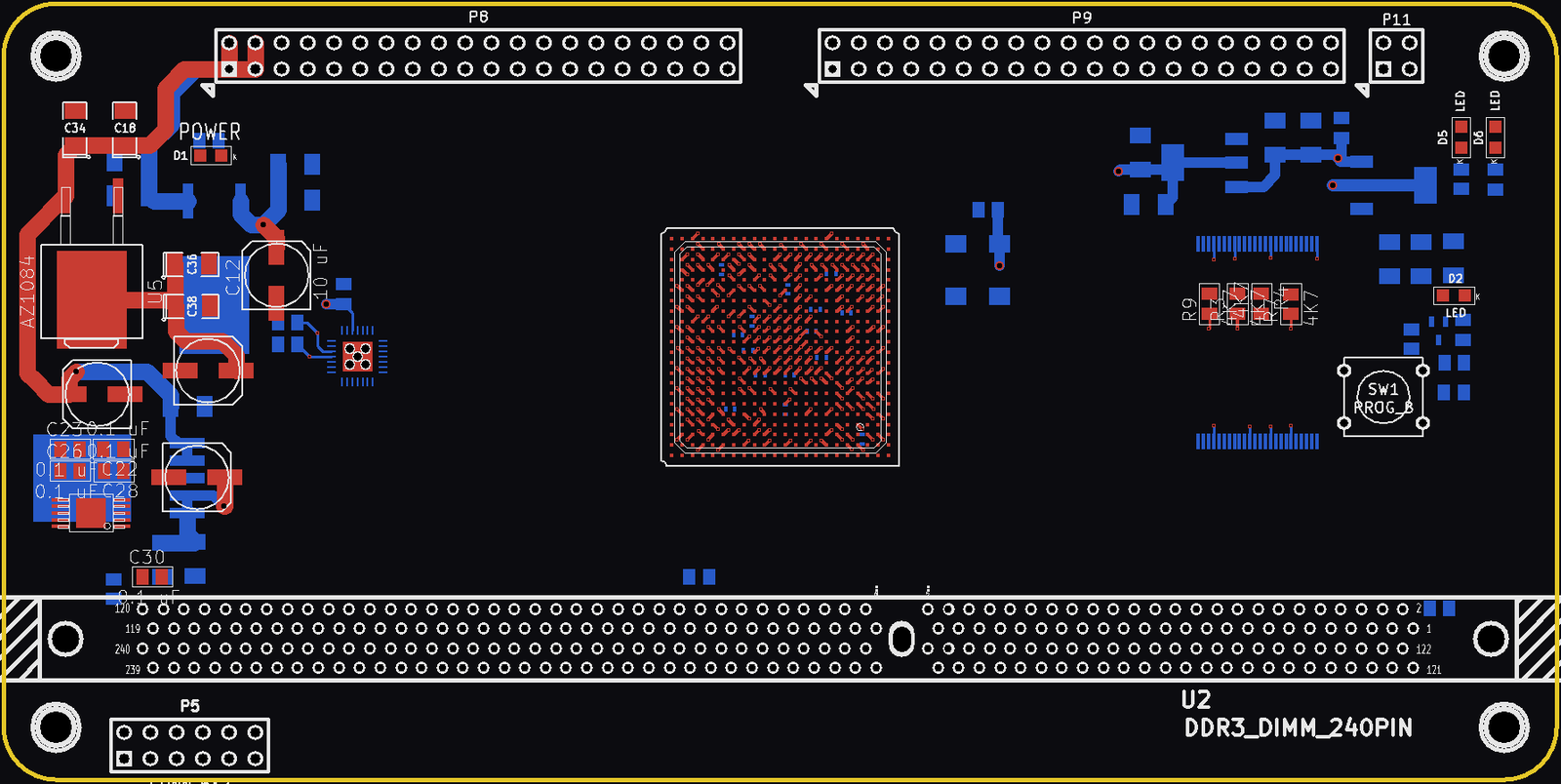
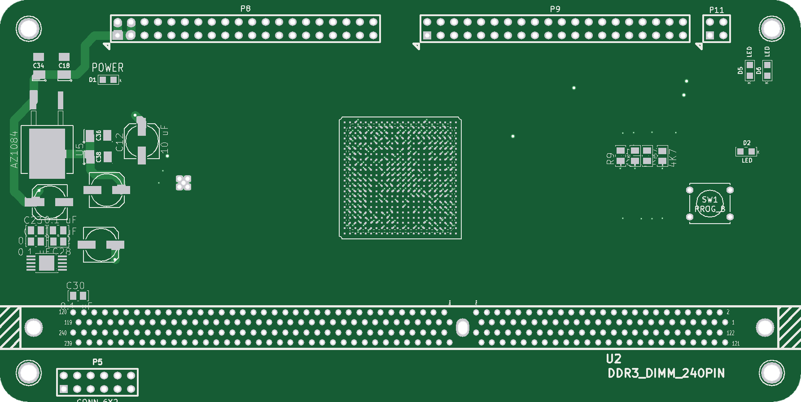
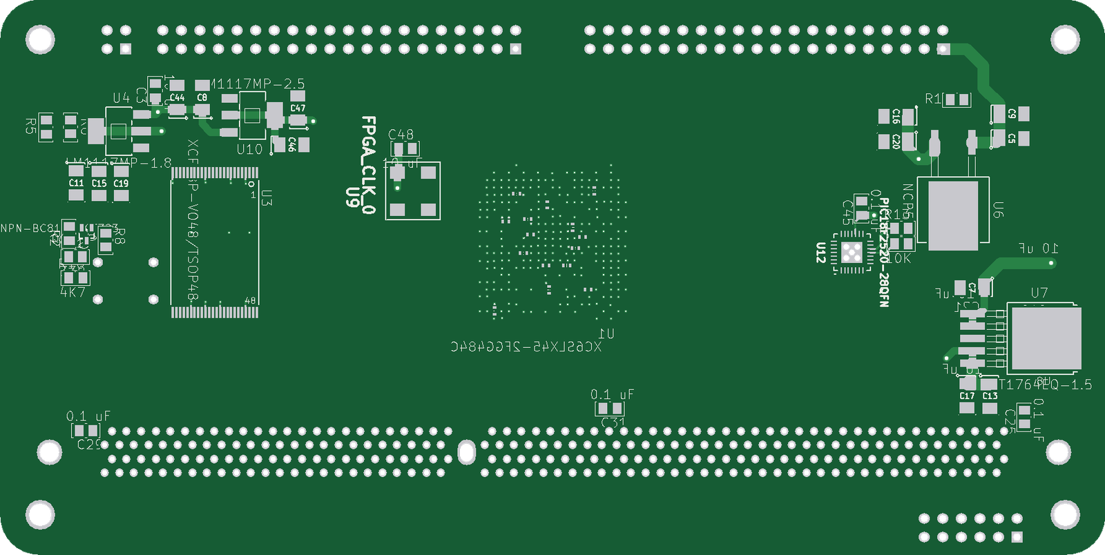
Unfinished: schematic and placed, partly routed PCB only. It was never routed or built.
GERBERS/ folder in the original project is empty.| Ref | Part | Role |
|---|---|---|
| U1 | XC6SLX45-2FGG484C | FPGA, DDR3 interface to the adapter board |
| U2 | 240-pin DDR3 DIMM socket | 64-bit unbuffered DIMM, 2 ranks |
| U3 | XCF08P (TSOP48) | FPGA configuration flash |
| U12 | PIC18F2520 (QFN28) | on the DIMM SPD I2C bus, 6 lines to the FPGA |
| U9 | oscillator | FPGA clock into ball M3 (GCLK); a 62.5 MHz 2.5 V part in digikey.xlsx |
| U5 | AZ1084 | 3.3 V from +8 V |
| U6 | NCP565 | 1.2 V (FPGA core) |
| U7 | LT1764EQ-1.5 | 1.5 V DIMM supply |
| U8 | RT9026 | DDR3 VTT / VREF |
| U4, U10 | LM1117-1.8, LM1117-2.5 | XCF08P core, oscillator |
| P8, P9 | 2x20 headers | to the x86 32bit Memory Adapter Board |
| P11 | 2x2 header | JTAG (TDI, TDO, TMS, TCK) |
| P5 | 2x6 header | PIC programming (MCLR/PGD/PGC) and UART (TX/RX) |
| SW1 | push button | FPGA PROG_B |
| D1, D2 | LEDs | POWER, FPGA DONE (via Q1) |
| File | What it is |
|---|---|
4Mem board v2.sch | schematic (single sheet) |
4Mem board v2-cache.lib | symbol cache |
4Mem board v2.kicad_pcb | PCB (placed, partly routed) |
4Mem board v2.pro | KiCad project |
4Mem board v2.net, .cmp | netlist and footprint assignments |
digikey.xlsx | DigiKey parts list (NZD), including parts for the sibling SRAM/adapter boards |
There is no FPGA project for this board.
.dsn) export of the same PCB on 2016-12-06. It isn't included./V1.2temp, /V1.5temp and /V3.3temp are not joined to the regulator outputs /V1.2, /V1.5 and /V3.3./+8Vitemp, the input to U4 and U10, is not joined to /+8Vi./V3.3temp2./DDR3_OFT1 is the DIMM ODT1 signal.Hardware: CERN-OHL-S-2.0 for the original work in this folder; see the repo NOTICE for third-party parts.
| Qty | Value | Footprint | References |
|---|---|---|---|
| 26 | 330 | ^^SMD_Resistor-0805 | R1, R13, R14, R15, R16, R20, R21, R22, R23, R24, R29, R31, R33, R35, R37, R39 +10 |
| 11 | 0.1 uF | C2 | C3, C4, C6, C8, C17, C20, C21, C25, C27, C28, Cx15 |
| 11 | 470 | ^^SMD_Resistor-0805 | R2, R7, R18, R19, R28, R32, R34, R36, R38, R46, R47 |
| 10 | C | ^^SMD_Resistor-0805 | C19, C26, C33, C34, C35, C36, C37, C38, C39, C40 |
| 10 | JUMPER | PIN_ARRAY_2X1 | JP4, JP5, JPx1, JPx2, JPx3, JPx4, JPx5, JPx6, JPx7, JPx8 |
| 9 | ^^NPN-SOT23 | ^^-SOT23 | Q1, Q2, Q3, Q4, Q5, Q6, Q7, Q8, Q9 |
| 7 | ^^74LS541 | ^^-SO20W | U3din1, U3dout1, U4, U5, U6, U11, U19 |
| 6 | 10 uF | C1V7 | C1, C2, C5, C7, C11, C12 |
| 5 | 10k | ^^SMD_Resistor-0805 | R4, R8, R10, R11, R30 |
| 4 | LED | ^^LED-0805 | D1, D4, Dx2, Dx3 |
| 3 | 100 | ^^SMD_Resistor-0805 | R25, R26, R27 |
| 3 | 10K | ^^SMD_Resistor-0805 | R9, R12, R17 |
| 3 | M25P80 | -SO8 | U15, U16, U17 |
| 2 | 15 pF | ^^SMD_Resistor-0805 | C10, C18 |
| 2 | 74HC245 | ^^-SO20W | U7a1, U7b1 |
| 2 | CONN_1 | 1pin | P6, P7 |
| 2 | CONN_2 | ^^SMD_Resistor-0805 | P8, P9 |
| 2 | CONN_4 | SIL-4 | P2, P10 |
| 2 | RESET | SW_PUSH_SMALL | SW1, SW2 |
| 2 | USB_2 | USB_A | Jx1, Jx2 |
| 1 | 0.01 uF | ^^SMD_Resistor-0805 | C15 |
| 1 | 0.1 uF | ^^SMD_Resistor-0805 | C14 |
| 1 | 12MHz | Crystal_HC-49U_Vert | X1 |
| 1 | 16550 | DIP-40__600_ELL | Ux18 |
| 1 | 1K | ^^SMD_Resistor-0805 | R3 |
| 1 | 22 uF | C1V7 | C9 |
| 1 | 4700 | ^^SMD_Resistor-0805 | Rx2 |
| 1 | 74LS682N | 20DIP-ELL300 | Ux17 |
| 1 | BOARD_SELECT | ^^LED-0805 | D7 |
| 1 | CH341A | -SO28W | U18 |
| 1 | CLK_UART | DIP-14__300_ELL | Px12 |
| 1 | CONN_2 | SIL-2 | P3 |
| 1 | CONN_3 | SIL-3 | Kx1 |
| 1 | DIPS_08 | 16dip300 | SWx2 |
| 1 | DONE | ^^LED-0805 | D6 |
| 1 | FLASH/RUN | SW_PUSH_SMALL | SW50 |
| 1 | FLASH_0 | ^^LED-0805 | D9 |
| 1 | FLASH_1 | ^^LED-0805 | D10 |
| 1 | FLASH_2 | ^^LED-0805 | D11 |
| 1 | FLASH_3 | ^^LED-0805 | D12 |
| 1 | FLASH_SELECT | SW_PUSH_SMALL | SW4 |
| 1 | FT232R | -SSOP28 | Ux21 |
| 1 | LDO_REG_7805 | ^^TO220 | U1 |
| 1 | LM1086CS | ^^TO220 | U2 |
| 1 | M25P80 | 8DIP-ELL300 | U14 |
| 1 | M25P80 ISP | SIL-5 | P1 |
| 1 | P54 | ^^LED-0805 | D3 |
| 1 | P55 | ^^LED-0805 | D2 |
| 1 | PIC18F1330 | -SO18-1 | U8 |
| 1 | PIC_ISP | SIL-6 | P5 |
| 1 | POWER | ^^LED-0805 | D5 |
| 1 | POWER CH341A | ^^LED-0805 | D8 |
| 1 | POWER FT232R | ^^LED-0805 | D13 |
| 1 | S100_MALE | S100_MALE | P4 |
| 1 | TMA0 | ^^LED-0805 | D14 |
| 1 | TMA1 | ^^LED-0805 | D15 |
| 1 | TMA2 | ^^LED-0805 | D16 |
| 1 | TMA3 | ^^LED-0805 | D17 |
| 1 | XC95288XL-TQ144 | -TQFP144 | U20 |
| 1 | XILINX CABLE2 | PIN_ARRAY_5x2 | P19 |
| 1 | ^^3.3VREG_SOT223 | -SOT223 | Ux1 |
| 1 | ^^74LV244 | ^^-SO20W | U12 |
CatspersCoffee/S100-Boards
S-100 bus boards designed and built: Z80 and 80386 CPU cards, SRAM/DRAM memory, CPLD/FPGA I/O and SPI boards, an 18-slot backplane and bus terminator.

CatspersCoffee/S100-Boards
S-100 bus boards designed and built: Z80 and 80386 CPU cards, SRAM/DRAM memory, CPLD/FPGA I/O and SPI boards, an 18-slot backplane and bus terminator.

CatspersCoffee/S100-Boards
S-100 bus boards designed and built: Z80 and 80386 CPU cards, SRAM/DRAM memory, CPLD/FPGA I/O and SPI boards, an 18-slot backplane and bus terminator.

CatspersCoffee/S100-Boards
S-100 bus boards designed and built: Z80 and 80386 CPU cards, SRAM/DRAM memory, CPLD/FPGA I/O and SPI boards, an 18-slot backplane and bus terminator.

CatspersCoffee/S100-Boards
S-100 bus boards designed and built: Z80 and 80386 CPU cards, SRAM/DRAM memory, CPLD/FPGA I/O and SPI boards, an 18-slot backplane and bus terminator.

CatspersCoffee/S100-Boards
S-100 bus boards designed and built: Z80 and 80386 CPU cards, SRAM/DRAM memory, CPLD/FPGA I/O and SPI boards, an 18-slot backplane and bus terminator.

CatspersCoffee/S100-Boards
S-100 bus boards designed and built: Z80 and 80386 CPU cards, SRAM/DRAM memory, CPLD/FPGA I/O and SPI boards, an 18-slot backplane and bus terminator.

CatspersCoffee/S100-Boards
S-100 bus boards designed and built: Z80 and 80386 CPU cards, SRAM/DRAM memory, CPLD/FPGA I/O and SPI boards, an 18-slot backplane and bus terminator.


Upcycle-Electronics/CH341A-Pro
Retrace pics and schematic for the Cheap Black CH341A Serial Flash EEPROM BIOS Programmer

AliceAch/SPIN-FV1-Tone-Dev
A PCB Tone Development board for Guitar Effects, built around the SPIN FV1 DSP IC.

Omarbelh/FlashCore
Hybrid USB-C SPI Flash & EEPROM programmer based on CH341A and ESP32-S3.

ADBeta/CH341A_USB_C
USB-C CH341A Breakout Board with EEPROM, I2C, SPI and UART Outputs - with headers for SOIC Clips

It measures 254 × 134.1 mm and has 2 copper layers, 1.6 mm thick.
164 parts, built around the PIC18F1330-E/P, 74HC245D, 74LV244D and CH341A. The full list of its parts is on this page, with links to each part's symbol and footprint where PCBKit's library has them.
From the CatspersCoffee/S100-Boards repository on GitHub, at the commit this page was made from: the board is Flash-UART/S100_B1FU.kicad_pcb. PCBKit opens the board in the browser, with nothing to install.
Its repository states no licence, so its author keeps all rights: ask CatspersCoffee before reusing the design.