Skip to the content
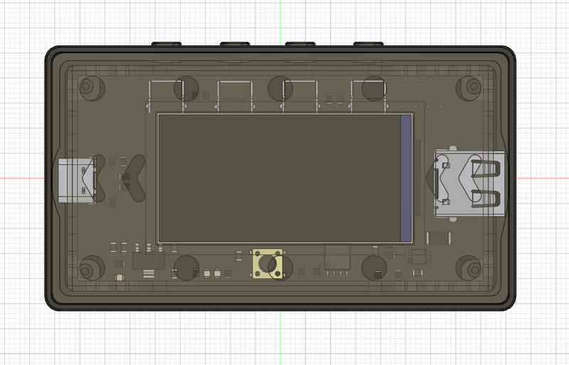
2 layers86 × 45 mmStm32f103, the printed circuit board in 3D

【USB功率计】PowerWatch 自制的 USB 电源功率计,用于测量具备 USB 接口的设备输出电能参数,支持测量电压(V),电流(A),功率(W),电能(Ah, Wh)

Size
86 × 45 mm
Copper layers
2
Thickness
1.6 mm
Parts
61
Nets
84
Pads
259
Tracks, vias
514, 52
Pours
192
Routed
Yes
KiCad
KiCad 6 (file 20211014)
Created
13 May 2022
Updated
26 Aug 2025

Overview

Stm32f103 is an open-source printed circuit board by zhbi98, from the zhbi98/PowerWatch repository on GitHub, published under the MIT licence. It is a 2-layer board of 86 × 45 mm with 61 parts on 84 nets, routed with 514 tracks and 52 vias.

It is built around the INA226AIDGSR, W25Q32JVSSIQ and LM1117-3.3, with the USB4105-GF-A among its other parts. Its parts include 24 resistors, 13 capacitors, 6 connectors, 5 switches and 4 ICs. It belongs with the STM32 boards of this library.

Main components

4

README

README.md

PowerWatch 迷你 USB 电源功率计

1. 项目简介

PowerWatch 是我设计的一个 Mini-USB 电源功率计,设计包含外观结构,电路 PCB,程序固件。

PowerWatch 在硬件设计上支持同时采样被测电源的电压,电流及功率等参数,同时通过软件的形式实现了电能实时监测功能。

电能实时监测功能可以方便的知道被监测电源所输出的电能。 比如通过 PowerWatch 可以知道充电宝为手机充电时,充电宝流入手机的电能为多少 mAh。

而其中 mAh 表明的是电能单位,例如以 $x$ mA 电流持续输出 $1$ h 时间,则输出的电能为 $x$ mAh。

2. 硬件介绍

(1) 微控制器:采用国产兆易 GD32F103RCT6,芯片主频 96MHz 最高可达 108MHz,64P 引脚,RAM 空间 64KB,ROM 空间 256KB,支持 USB 通信。

(2) 屏幕:驱动芯片 ST7789V3,材质 IPS,采用 8 位并行 8080 通信接口,分辨率 320x170。

(3) Flash 芯片:GD25Q64 64MBit 即 8MByte。

(4) 电压电流采样芯片:采用德州仪器 TI 的 INA226AIDGSR 芯片。

(5) 外壳模型:3D 打印,材料使用尼龙或工程塑料 。

3. 目录说明

3.1 Firmware 目录

该目录包含 PowerWatch 的所有功能源码实现,芯片驱动库,以及 Keil 编译工程所在目录,现在来简单介绍一下。

mdk5/ 目录即为 MDK-ARM(即 Keil5 集成开发环境) 的工程文件。

test/ 目录包含所有功能实现源码,以及需要用到的芯片驱动库,图形界面库 LVGL。

程序主要包含以下内容:

(1) GD32f103 的 USB Device 设备驱动,USB 驱动使用的设备描述符是 CDC 虚拟串口,使用 USB 接口可以用于和上位机进行数据通讯。

(2) ST7789V3 屏幕芯片驱动。

(3) 电压电流采样芯片驱动。

(4) 移植好的 LVGL8.2.0 的 UI 绘图库,这个 UI 库可以实现美观的图形界面,使用 LVGL 后就不需要我们自己控制屏幕逐像素的绘制图形来实现 UI 了。

注意:如果需要编译此工程需要安装 keil5 集成开发环境,以及在 keil5 中安装 GD32F10 系列的芯片描述包, 安装好后点击本项目工程文件夹下的工程文件启动 keil 直接编译即可。

GD32F10 芯片描述包可以到兆易官方网站下载,找到 GD32F1x0 AddOn 压缩包,芯片描述包就在该压缩包下,下载地址:点击这里。


power_watch_firmware_v1.0.hex:为 PowerWatch 源码的编译后的固件,如果使用编译固件,需要使芯片进入 BOOT 模式,并使用 PCB 板上预留的串口来写入该固件。

3.2 Hardware 目录

PowerWatch 的 PCB 工程源文件,该文件夹下包含电路原理图,以及 PCB 制造文件(即 Gerber 文件),器件 BOM 单(用于 SMT 贴片),器件位置文件(用于 SMT 贴片)。

将 Gerber 文件压缩后到嘉立创网站下单即可将 PCB 打样出来,BOM 单和器件位置文件是嘉立创格式,PCB 打样后可以自行按照 BOM 单购买元器件手工焊接,或利用我提供的 BOM 单和器件坐标文件运用嘉立创的 SMT 贴片服务来贴片。

硬件 PCB 已经打样验证通过,想制作的小伙伴可以放心打样使用。


PCB 设计时原本的设想是使用 STM32F103RCT6 这颗芯片作为微控制器使用的,但是奈何 STM32F103RCT6 价格较高,所以最终芯片使用的是国产兆易的 GD32F103RCT6 系列芯片。

但是这对电路并不影响,因为 GD32F103RCT6 可以不需要任何改动而实现 PIN 对 PIN 的引脚以及外设兼容 STM32F103RCT6 芯片(即它们的每一根引脚和外设的功能是相同的)。

3.3 Image 目录

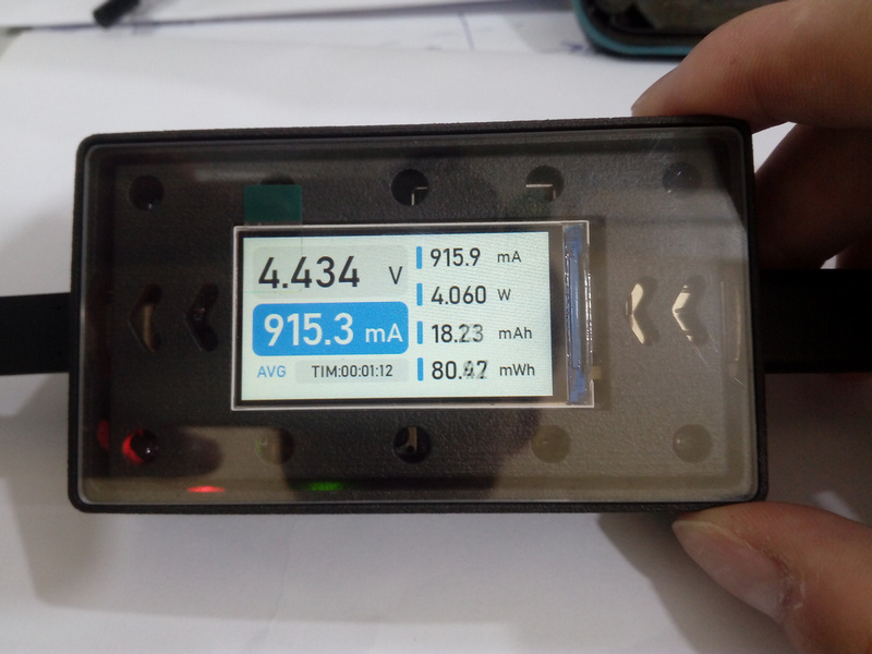
该目录是功率计制作实物效果图片展示,观看制作效果可以查看该目录下的实物照片。

3.4 Structure 目录

该目录存放功率计外壳模型文件 .step 格式,外壳模型包含壳体,按键帽,屏幕支架,上盖板,直接下载用于 3D 打印即可。

为了美观考虑盖板最好使用透明亚克力板进行制作,普通 3D 打印无法实现透明。

(1) 壳体 box_v2.0.step 建议采用黑色尼龙材材料 3D 打印。

(2) 屏幕支架 bracket_v2.0.step 建议采用透明树脂材料 3D 打印。

(3) 上盖板 panel_v2.0.step 建议采用亚克力或聚碳酸酯材料 CNC 加工。

(4) 按键帽 button1_v2.0.step,button2_v2.0.step,button3_v2.0.step,button4_v2.0.step 建议采用尼龙材料 3D 打印。

3.5 Docs 目录

用到的芯片配套的数据手册。

4. 外观设计

最初的 V1.0 版本模型效果
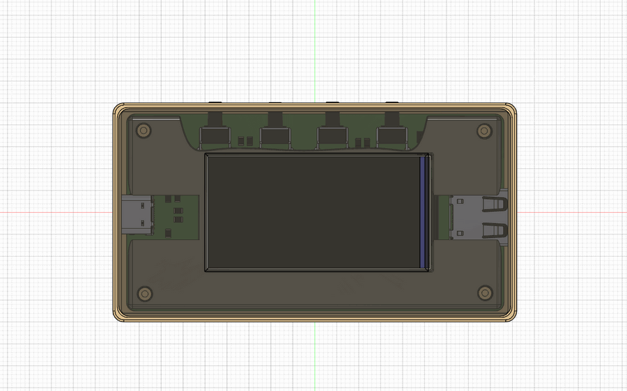
image.png

改进后 V2.0 版本模型效果

image.png

5. 实物展示

image.png

Parts

61
QtyValueFootprintReferences
90.1uFCapacitor_SMD:C_0805_2012MetricC3, C6, C7, C8, C9, C10, C11, C12, C13
65.1KResistor_SMD:R_0805_2012MetricR16, R17, R18, R19, R20, R21
5220RResistor_SMD:R_0805_2012MetricR1, R2, R3, R4, R14
41-1825027-13rd_Button_Switch_THT:KEY-TH_L6.0-W6.0-H_B3F-3100S1, S2, S3, S4
410KResistor_SMD:R_0805_2012MetricR6, R10, R22, R24
4Mounting_Holes_3mm_THTZhbi_Mounting_Holes:Mounting_Holes_3mm_THTM1, M2, M3, M4
20.5KResistor_SMD:R_0805_2012MetricR7, R8
210uFCapacitor_SMD:C_0805_2012MetricC2, C5
220RResistor_SMD:R_0805_2012MetricR11, R12
222pFCapacitor_SMD:C_0805_2012MetricC1, C4
1100RResistor_SMD:R_0805_2012MetricR23
1100mRResistor_SMD:R_2010_5025MetricR15
110MResistor_SMD:R_0805_2012MetricR5
11825910-63rd_Button_Switch_THT:KEY-TH_L6.0-W6.0-V_B3F-1000SW1
11KResistor_SMD:R_0805_2012MetricR13
11kResistor_SMD:R_0805_2012MetricR9
18MCrystal:Crystal_SMD_HC49-SDY1
1Conn_01x30Connector_FFC-FPC:Hirose_FH12-30S-0.5SH_1x30-1MP_P0.50mm_HorizontalJ4
1INA226 ALERTConnector_PinSocket_2.54mm:PinSocket_1x01_P2.54mm_VerticalJ5
1INA226AIDGSR3rd_Sensor_Power:VSSOP-10_L2.9-W5.05-P0.5_INA226AIDGSRU3
1LED1LED_SMD:LED_0805_2012MetricD2
1LED2LED_SMD:LED_0805_2012MetricD3
1LM1117-3.3Package_TO_SOT_SMD:SOT-223U1
1POWER LEDLED_SMD:LED_0805_2012MetricD1
1Q_PNP_BECPackage_TO_SOT_SMD:SOT-23Q1
1STM32F103RCTxPackage_QFP:LQFP-64_10x10mm_P0.5mmU2
1SWDConnector_PinSocket_2.54mm:PinSocket_1x04_P2.54mm_VerticalJ1
1USART1Connector_PinSocket_2.54mm:PinSocket_1x03_P2.54mm_VerticalJ2
1USB1130-15-A_REVA3rd_Connector_USB:USB-A-TH_4P_USB1130-15-A-REVAJ6
1USB4105-GF-A3rd_Connector_USB:USB-C-SMD_16P_USB4105-GF-AJ3
1W25Q32JVSS3rd_Memory_Flash:SOIC-8_L4.8-W5.8-P1.27_W25Q32JVSSU4

Similar boards

  • 4 layers58.1 × 62.5 mmFirst try, the printed circuit board in 3D

    First try

    usunwshineu/Low_Power_FPGA_PCB

    A custom low-power FPGA development board based on the Lattice iCE40UP5K FPGA. The board was designed to provide FPGA processing capabilities together with power monitoring and common communication interfaces.

    136 parts
  • 8 layers153.7 × 88.9 mmLink, the printed circuit board in 3D

    Link

    oro-os/link

    The Oro OS CI/CD pipeline including PCBs, CAD files, firmware and server infrastructure

    381 parts14MIT
  • 4 layers96.5 × 85.5 mmSense&ControlBoard, the printed circuit board in 3D

    Sense&ControlBoard

    Ben-Bussch/COMET-I-Static-Fire

    Avionics for Static Fire of Comet 1

    147 parts
  • 4 layersDA37 power C, the printed circuit board in 3D

    DA37 power C

    Fairank/WhisperTorch

    声束手电 · A directional-audio engineering prototype with editable KiCad PCBs, a serviceable 3D-printable enclosure and ESP32/Pico firmware. Source-available for noncommercial use; range targets remain unverified.

    83 parts
  • 4 layers22.9 × 61 mmPico ice, the printed circuit board in 3D

    Pico ice

    tinyvision-ai-inc/pico-ice

    Raspberry Pi PICO board + Lattice iCE40 FPGA's

    109 parts203MIT
  • 4 layers27.9 × 63.5 mmPico2-ice, the printed circuit board in 3D

    Pico2-ice

    tinyvision-ai-inc/pico2-ice

    Doc | Hardware | SDK | Schematic | Assembly | Discord

    124 parts60MIT
  • 2 layers225 × 63.5 mmGnss-7-seg clock, the printed circuit board in 3D

    Gnss-7-seg clock

    Tosainu/gnss-7-seg-clock

    GNSS-powered, seven-segment table clock

    90 parts6MIT
  • 2 layers89 × 83 mmPico2-nx, the printed circuit board in 3D

    Pico2-nx

    tinyvision-ai-inc/pico2-nx

    RP2350+Lattice Crosslink NX FPGA board

    242 parts5MIT

Questions

How big is the Stm32f103 PCB?

It measures 86 × 45 mm and has 2 copper layers, 1.6 mm thick.

What parts does the Stm32f103 use?

61 parts, built around the INA226AIDGSR, W25Q32JVSSIQ, LM1117-3.3 and USB4105-GF-A. The full list of its parts is on this page, with links to each part's symbol and footprint where PCBKit's library has them.

Where can I download the Stm32f103 KiCad files?

From the zhbi98/PowerWatch repository on GitHub, at the commit this page was made from: the board is Hardware/kicad_project/stm32f103.kicad_pcb and its schematic Hardware/kicad_project/stm32f103.kicad_sch. PCBKit opens the board in the browser, with nothing to install.

Can I use the Stm32f103 design in my own project?

Its repository publishes it under the MIT licence: you may reuse it on that licence's terms (keep the author's notice, and for a copyleft licence share your changes alike).