2 layers76.5 × 78 mm
EmonTH
openenergymonitor/emonTH3
Hardware for the emonTH3 temperature, humidity, and pulse sensing node
56 partsCC-BY-SA-4.0
 ytr0/mkctrl-v2
DIYゲームコントローラー制作ツールキット
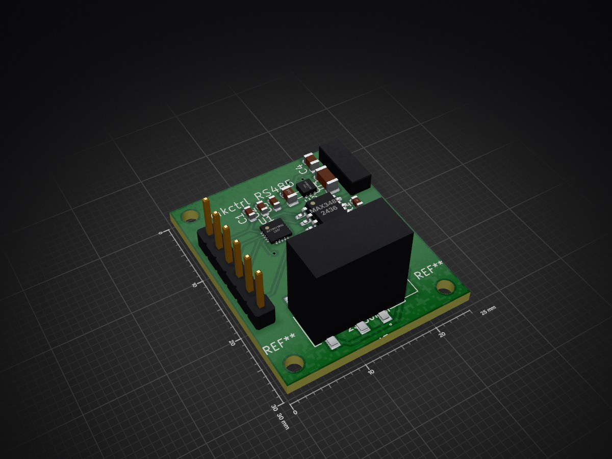
Attiny rs485 is an open-source printed circuit board by ytr0, from the ytr0/mkctrl-v2 repository on GitHub. It is a 2-layer board of 25 × 30 mm with 16 parts on 14 nets, routed with 78 tracks and 5 vias.
It is built around the ATTINY1616-MN, MAX3485ED and RS485, with the TPS61291DRV among its other parts. Its parts include 5 capacitors, 3 ICs, 3 connectors, 1 resistor and 1 inductor. It belongs with the interfaces and adapters boards and the AVR (ATmega, ATtiny) boards of this library.


Version: v2.5.1.2026.0401 KiCad: 8.0+ Status: 設計完了、製造待ち
外部ジョイスティック/センサをRS485経由でM5AtomS3に接続するための小型入力モジュール。
┌─────────────────────────────┐      RS485       ┌───────────────┐
│   ATtiny1616 RS485 Module   │ ═══════════════> │  M5AtomS3 #1  │
│                             │   115200bps      │   (Sensor)    │
│  ┌─────────┐  ┌─────────┐   │   ~100m max      └───────┬───────┘
│  │Joystick │  │ Button  │   │                          │
│  │  X / Y  │  │         │   │                     ESP-NOW
│  └────┬────┘  └────┬────┘   │                      ~2ms
│       │            │        │                          │
│       ▼            ▼        │                          ▼
│  ┌──────────────────────┐   │                  ┌───────────────┐
│  │    ATtiny1616        │   │                  │  M5AtomS3 #2  │
│  │    ADC + UART TX     │   │                  │  (Receiver)   │
│  └──────────┬───────────┘   │                  └───────┬───────┘
│             │               │                          │
│             ▼               │                      USB Serial
│  ┌──────────────────────┐   │                      2Mbps
│  │      MAX3485         │   │                          │
│  │   RS485 Transceiver  │───┼──────────────────────────┘
│  └──────────────────────┘   │                          ▼
│                             │                  ┌───────────────┐
│   [3.3V]    [GND]           │                  │  Processing   │
└─────────────────────────────┘                  │    + OSC      │
       ↑                                         └───────┬───────┘
       │                                                 │
外部電源 UE5/Game| 項目 | 値 | 備考 |
|---|---|---|
| 動作電圧 | 3.3V | 2.7V〜5.5V対応(ATtiny1616) |
| 消費電流(アクティブ) | ~10mA | ADC + RS485送信時 |
| 消費電流(アイドル) | ~2mA | 送信停止時 |
| 消費電流(スリープ) | ~0.3mA | パワーダウンモード |
| クロック | 20MHz | 内蔵RC |
| 項目 | 値 | 備考 |
|---|---|---|
| プロトコル | RS485 半二重 | 送信専用 |
| ボーレート | 115200 bps | |
| ポーリングレート | 100Hz | 10ms間隔 |
| フレーム | 8N1 | |
| CRC | CRC-16-CCITT | |
| 最大ケーブル長 | ~100m | 終端抵抗使用時 |
100Hzは以下の比較から十分と判断:
| コントローラ | ポーリングレート |
|---|---|
| PS5 DualSense | 250Hz (USB) |
| Xbox Series | 125Hz |
| Switch Pro | 60Hz |
| 本設計 | 100Hz |
単三電池(AA)1本(1.5V)での駆動を検討:
| 条件 | 推定駆動時間 | 備考 |
|---|---|---|
| 連続アクティブ | ~50時間 | 2500mAh × 0.85効率 ÷ ~45mA |
| 50%アクティブ | ~85時間 | アイドル時省電力 |
| スリープ多用 | ~2ヶ月 | ウェイクオン入力で復帰 |
要件:
注意: 現行基板は外部3.3V電源を想定。電池駆動版は別途設計が必要。
| Ref | 部品 | パッケージ | 値 | 備考 |
|---|---|---|---|---|
| U1 | ATtiny1616-MNR | QFN-20 (3x3mm) | - | MCU |
| U2 | MAX3485ED | SOIC-8 | - | RS485トランシーバ |
| C1 | セラミックコンデンサ | 0603 | 100nF | U1デカップリング |
| C2 | セラミックコンデンサ | 0603 | 100nF | U2デカップリング |
| C3 | セラミックコンデンサ | 0603 | 10µF | 電源バルク |
| R1 | 抵抗 | 0603 | 1kΩ | LED電流制限 |
| R2 | 抵抗 | 0603 | 10kΩ | PB0プルダウン |
| R3 | 抵抗 | 0603 | 10kΩ | PB1プルダウン |
| R4 | 抵抗 | 0603 | 10kΩ | PA3プルアップ(内蔵使用なら省略可) |
| D1 | LED | 0603 | 緑 | ステータス |
| J1 | ピンヘッダ | 2.54mm 2x3 | - | センサ接続 |
| J2 | ピンヘッダ | 2.54mm 1x2 | - | RS485 (A/B) |
| J3 | ピンヘッダ | 2.54mm 1x2 | - | 電源 (VCC/GND) |
| J4 | ピンヘッダ | 2.54mm 1x3 | - | UPDI (VCC/UPDI/GND) |
| J5 | 3.5mmジャック | PJ-320D SMD | - | RS485 (T=A, R1=B, S=GND) |
                                    VCC (3.3V)
                                       │
                                      ┌┴┐
                                      │ │ R4 10k (optional)
                                      └┬┘
          ┌─────────────────────────┐  │
          │      ATtiny1616-MNR     │  │
          │                         │  │
    VCC ──┤1  VCC           PA3  16├──┴── BTN (J1)
          │                         │
   UPDI ──┤2  PA0/UPDI      PA2  15├────── (NC)
          │                         │
          │3  PA1/TX        PA1  14├────── (see PA1/TX)
          │                         │
          │4  PA2           GND  13├────── GND
          │                         │
    GND ──┤5  GND           PA7  12├──┬── LED ──[R1 1k]── GND
          │                         │  │
          │6  PB5           PA6  11├──┼── DE/RE (U2)
          │                         │  │
          │7  PB4           PA5  10├──┼── (NC - RX unused)
          │                         │  │
  B0/S1 ──┤8  PB3           PA4   9├──┼── (NC)
│ │ │ ┌──────────────────┐
│ 20 19 18 17 16 │
│ ○ │
1 │ │ 15
2 │ │ 14
3 │ ATtiny1616 │ 13
4 │ -MNR │ 12
5 │ │ 11
│ 6 7 8 9 10 │
└──────────────────┘
(PAD = GND)
Pin 1: VCC
Pin 2: PA4
Pin 3: PA5
Pin 4: PA6 → DE/RE (MAX3485)
Pin 5: PA7 → LED (via R1)
Pin 6: PB3 → (NC)
Pin 7: PB2 → (NC)
Pin 8: PB1 → ADC B1 (via R3 pulldown)
Pin 9: PB0 → ADC B0 (via R2 pulldown)
Pin 10: PC3 → (NC)
Pin 11: PC2 → (NC)
Pin 12: PC1 → (NC) ┌───────┐
RO ─┤1 8├─ VCC (3.3V)
/RE ─┤2 7├─ B (RS485-)
DE ─┤3 6├─ A (RS485+)
DI ─┤4 5├─ GND
└───────┘
接続:
- Pin 1 (RO): NC (受信未使用)
- Pin 2 (/RE): PA6 (DE と共通)
- Pin 3 (DE): PA6
- Pin 4 (DI): PA1 (TX)
- Pin 5 (GND): GND
- Pin 6 (A): RS485 A (+)
- Pin 7 (B): RS485 B (-)
- Pin 8 (VCC): 3.3VVCC ──┬──[C3 10µF]──┬── GND
│ │
├──[C1 100nF]─┤ (U1近傍)
│ │
└──[C2 100nF]─┘ (U2近傍)PB0 ──┬── センサ入力
│
[R2 10kΩ]
│
GND
PB1 ──┬── センサ入力
│
[R3 10kΩ]
│
GND| 項目 | 値 |
|---|---|
| サイズ | 25mm x 30mm |
| 層数 | 2層 |
| 板厚 | 1.6mm |
| 銅箔厚 | 35µm (1oz) |
| 表面処理 | HASL or ENIG |
| レジスト | 緑 |
| シルク | 白 |
以下は0 DRCエラーを達成した最終レイアウト。座標は基板左下原点(0,0)からのmm値。
Y=0    ──────────────────────────
       │                        │
Y=3.5  │  J1(3.5)      J3(17)   │  ← 上部ヘッダ
       │  Sensor       Power    │
       │  2x3          1x3      │
       │                        │
Y=8    │          C1(10)        │  ← 100nF (U1用)
       │                        │
Y=10   │          C2(10)        │  ← 100nF (U2用)
       │                        │
Y=12   │    R3(5)               │  ← 10k (ADC B1)
       │                        │
Y=13   │         ┌──────┐       │
Y=14   │  D1(5)  │ U1   │ R1(15)│  ← ATtiny1616 @ (10,13)
       │  LED    │(10,13)│ 1k   │
Y=16   │         └──────┘       │
       │       C3(10)  R2(13)   │  ← 10µF, 10k (ADC B0)
       │                        │
Y=17   │  J4(3)                 │  ← UPDI 1x3
       │  UPDI                  │
       │                        │
Y=20   │        ┌──────┐  J2(17)│  ← MAX3485 @ (10,20)
       │        │ U2   │  RS485 │
│ │(10,20)│ 1x2 │| Ref | 位置 (X, Y) mm | 部品 |
|---|---|---|
| J1 | (3.5, 3.5) | センサ 2x3 |
| J3 | (17.0, 3.5) | 電源 1x3 |
| C1 | (10.0, 8.0) | 100nF |
| C2 | (10.0, 10.0) | 100nF |
| R3 | (5.0, 12.0) | 10kΩ |
| U1 | (10.0, 13.0) | ATtiny1616 QFN-20 |
| D1 | (5.0, 14.0) | LED 緑 |
| R1 | (15.0, 14.0) | 1kΩ |
| C3 | (10.0, 16.0) | 10µF |
| R2 | (13.0, 16.0) | 10kΩ |
| J4 | (3.0, 17.0) | UPDI 1x3 |
| U2 | (10.0, 20.0) | MAX3485 SOIC-8 |
| J2 | (17.0, 20.0) | RS485 1x2 |
配置時は以下のコートヤード(部品周囲の禁止領域)を考慮:
| フットプリント | コートヤード幅 |
|---|---|
| 2x3 ピンヘッダ | X: 5.5mm, Y: 8.1mm |
| 1x3 ピンヘッダ | X: 3.0mm, Y: 8.1mm |
| 1x2 ピンヘッダ | X: 3.0mm, Y: 5.5mm |
| QFN-20 (3x3mm) | 5.0mm × 5.0mm |
| SOIC-8 | 6.0mm × 7.0mm |
| 0603 (R/C/LED) | 2.6mm × 1.6mm |
| 項目 | 最小値 |
|---|---|
| トラック幅 | 0.2mm |
| クリアランス | 0.2mm |
| ビア径 | 0.6mm |
| ビアドリル | 0.3mm |
| シルク幅 | 0.15mm |
自動配線ツール Freerouting を使用:
# DSNエクスポート(KiCad Python API経由)
/Applications/KiCad/KiCad.app/Contents/Frameworks/Python.framework/Versions/Current/bin/python3 << 'EOF'
import pcbnew
board = pcbnew.LoadBoard("attiny_rs485.kicad_pcb")
pcbnew.ExportSpecctraDSN(board, "attiny_rs485.dsn")
EOF

# Freerouting実行
java -jar freerouting-2.0.0.jar -de attiny_rs485.dsn -do attiny_rs485.ses -mp 100

# SESインポート
/Applications/KiCad/KiCad.app/Contents/Frameworks/Python.framework/Versions/Current/bin/python3 << 'EOF'
import pcbnew
board = pcbnew.LoadBoard("attiny_rs485.kicad_pcb")
pcbnew.ImportSpecctraSES(board, "attiny_rs485.ses")
pcbnew.SaveBoard("attiny_rs485.kicad_pcb", board)
EOF| 項目 | 値 |
|---|---|
| トレース数 | 48本 |
| ビア数 | 8個 |
| 配線層 | F.Cu(信号)、B.Cu(GND) |
| 配線時間 | ~2.4秒 |
Freerouting後、KiCad GUIで以下を実行:
Bキー| 部品 | シンボル | フットプリント |
|---|---|---|
| ATtiny1616-MNR | MCU_Microchip_ATtiny:ATtiny1616-MNR | Package_DFN_QFN:QFN-20-1EP_3x3mm_P0.4mm_EP1.65x1.65mm |
| MAX3485ED | Interface_UART:MAX3485E | Package_SO:SOIC-8_3.9x4.9mm_P1.27mm |
| 100nF | Device:C | Capacitor_SMD:C_0603_1608Metric |
| 10µF | Device:C | Capacitor_SMD:C_0603_1608Metric |
| 抵抗 | Device:R | Resistor_SMD:R_0603_1608Metric |
| LED | Device:LED | LED_SMD:LED_0603_1608Metric |
| ピンヘッダ 2x3 | Connector_Generic:Conn_02x03_Odd_Even | Connector_PinHeader_2.54mm:PinHeader_2x03_P2.54mm_Vertical |
| ピンヘッダ 1x2 | Connector_Generic:Conn_01x02 | Connector_PinHeader_2.54mm:PinHeader_1x02_P2.54mm_Vertical |
| ピンヘッダ 1x3 | Connector_Generic:Conn_01x03 | Connector_PinHeader_2.54mm:PinHeader_1x03_P2.54mm_Vertical |
| 3.5mmジャック | local:PJ-320D | local:PJ-320D (16.4x11.1mm SMD, 3D付) |
gerber/| Qty | Value | Footprint | References |
|---|---|---|---|
| 3 | 100nF | Capacitor_SMD:C_0603_1608Metric | C1, C2, C3 |
| 1 | 100uF | Capacitor_SMD:C_1206_3216Metric | C5 |
| 1 | 10uF | Capacitor_SMD:C_0805_2012Metric | C4 |
| 1 | 120R | Resistor_SMD:R_0603_1608Metric | R1 |
| 1 | 3.3uH | Inductor_SMD:L_0805_2012Metric | L1 |
| 1 | ATtiny1616 | Package_DFN_QFN:QFN-20-1EP_3x3mm_P0.4mm_EP1.65x1.65mm | U1 |
| 1 | MAX3485 | Package_SO:SOIC-8_3.9x4.9mm_P1.27mm | U2 |
| 1 | Power | Connector_PinHeader_2.54mm:PinHeader_1x03_P2.54mm_Vertical | J2 |
| 1 | RS485 | local:PJ-320D | J5 |
| 1 | Sensor | Connector_PinHeader_2.54mm:PinHeader_1x06_P2.54mm_Vertical | J4 |
| 1 | TPS61291 | Package_SON:WSON-6-1EP_2x2mm_P0.65mm_EP1x1.6mm | U3 |
The 13 most common of 16 parts.
It measures 25 × 30 mm and has 2 copper layers, 1.6 mm thick.
16 parts, built around the ATTINY1616-MN, MAX3485ED, RS485 and TPS61291DRV. The full list of its parts is on this page, with links to each part's symbol and footprint where PCBKit's library has them.
From the ytr0/mkctrl-v2 repository on GitHub, at the commit this page was made from: the board is hardware/attiny_rs485/attiny_rs485.kicad_pcb. PCBKit opens the board in the browser, with nothing to install.
Its repository states no licence, so its author keeps all rights: ask ytr0 before reusing the design.
openenergymonitor/emonTH3
Hardware for the emonTH3 temperature, humidity, and pulse sensing node

sifourquier/domotic_esp_hardware
hardware for a system based on esp8266

anyshake/explorer
🌏 Detecting seismic wave using 3 geophones and 3-axis accelerometer, pack & send data to AnyShake Observer over RS232 / RS485 serial.

fraxinas/DoorBirdPico
A custom Raspberry Pi Pico PCB design and code to add functionality to the DoorBird Voip entryphone.

austinscreations/Oxrs-Black
a custom rack controller that is based of the rack32 but includes some upgrades and major changes

bclswl0827/openstation
An open source, cross-platform, easy-to-use satellite automatic tracking system with hardware & software solutions.

ieb/BatterySensor
A Modbus RTU Battery Current and Voltage sensor board based Attiny3224, MAX485, MAX9918 chips.
