
6 layers141.7 × 105.1 mm
NuBoard
wickerwaka/nuBoard
Verified 2026-09-24 with KiCad 10.0.6. Open nuBoard.kicadpcb in this directory to inspect the result. This is a PCB-only candidate, separate from the main-board schematic and PCB.
330 parts1
 wickerwaka/nuBoard1
Verified 2026-09-24 with KiCad 10.0.6. Open nuBoard.kicadpcb in this directory to inspect the result. This is a PCB-only candidate, separate from the main-board schematic and PCB.
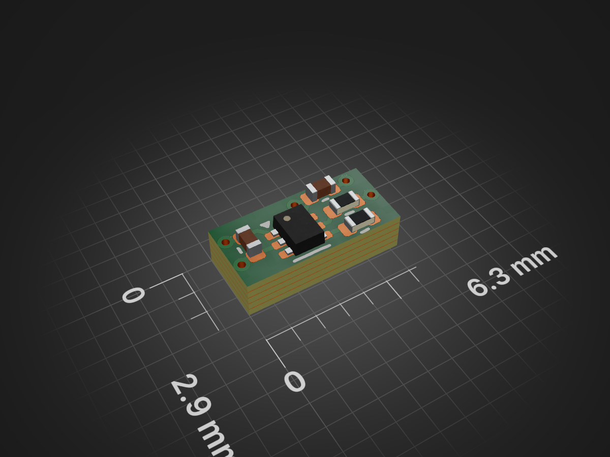
Clock Buffer is an open-source printed circuit board by wickerwaka, from the wickerwaka/nuBoard repository on GitHub. It is a 6-layer board with 5 parts on 7 nets, routed with 20 tracks and 5 vias.
It is built around the SN74LVC1T45DRL. Its parts include 2 capacitors, 2 resistors and 1 IC. It belongs with the lEDs and displays boards of this library.
Promoted to the main-board project on 2026-09-24. The authoritative
PCB is now ../../nuBoard.kicad_pcb, with its
schematic, pin-map CSV and displaced-signal FPGA constraints synchronized.
This directory remains the verified pre-promotion reference snapshot;
the description below records its original candidate status.
Verified 2026-09-24 with KiCad 10.0.6. Open nuBoard.kicad_pcb in this
directory to inspect the result. This is a PCB-only candidate, separate
from the main-board schematic and PCB. Do not update it from the unchanged
main schematic: its pin allocation is different.
U2 and all 585 HyperRAM signal track segments (DQ0–7, CK, RWDS, CS# and RESET#) are locked against accidental editing. U2's power connections are still unrouted; shared board power networks were not locked.
All ten required signals—CK, DQ0–7 and RWDS—are continuous, unbranched FPGA-pad-center to RAM-pad-center paths on F.Cu only, with zero vias. The PCB-only length spread is 0.214807 mm (8.457 mil), below the 0.381 mm (15 mil) limit by 0.166193 mm. No package compensation is configured. Unknown IC package skew is outside this approved requirement.
| Signal | FPGA ball | RAM ball | PCB length (mm) |
|---|---|---|---|
| DQ0 | K1 | D3 | 10.999998 |
| DQ1 | L1 | D2 | 10.999991 |
| DQ2 | H1 | C4 | 11.000001 |
| DQ3 | J1 | D4 | 11.000009 |
| DQ4 | G1 | D5 | 11.000003 |
| DQ5 | K2 | E3 | 11.000000 |
| DQ6 | L2 | E2 | 10.999998 |
| DQ7 | M3 | E1 | 10.999998 |
| CK | M1 | B2 | 11.000000 |
| RWDS | L3 | C3 | 11.214798 |
U2 remains on F.Cu at (90.8, 75.0) mm, 90°. No additional package movement or pin-map change from the last surface-routing trial was needed. CS# uses G3/A3 and RESET# uses G2/A4; their FPGA-to-RAM paths are also F.Cu-only without vias, but their pull-up branches remain unfinished.
The tuning patterns occupy the straight corridor between approximately x=93.3 and 99.0 mm. Coordinating their direction and spacing avoided the failed approach of inserting isolated large detours into crowded traces. CK and DQ0–7 target 11.0 mm; RWDS retains its original 11.214798 mm route. Trace width is 0.0762 mm, pattern period 0.44 mm, each bump's baseline width 0.22 mm, and corner bevel 0.01 mm. Bump counts for DQ0–7 are 9, 9, 2, 13, 3, 6, 10, 10 respectively; CK has one bump.
All 15 displaced signals retain the replacement routes documented in
hyperram-top-layer-plan.md.
Their nets have no unconnected items in the final DRC report.
drc.json: fresh DRC with copper zones refilled and the copied main-board
project/rules. No length-skew, shorting, clearance, hole-clearance or
courtyard violations. Six dangling-track warnings remain outside the
fast group, along with 27 whole-board unconnected items.verification.json: independent pad-to-pad graph/length audit, with
SHA-256 hashes of the checked PCB and DRC report. It checks both endpoint
identities, DDIO capability, RWDS clock capability, absence of branches,
disconnected copper and self-crossings, F.Cu-only routing, zero vias,
unset package compensation, and the ten-net maximum length spread.validation/test_hyperram_surface.py: mutation tests reject an open
segment, a via, a bottom-layer segment, excessive length, a dangling
branch and package compensation, even with the previously clean DRC.From the repository root, repeat:
kicad-cli pcb drc --refill-zones --format json \
  -o hardware/main-board/routing/hyperram-top/drc.json \
  hardware/main-board/routing/hyperram-top/nuBoard.kicad_pcb

# Use KiCad's Python environment (pcbnew and shapely are required).
python3 hardware/main-board/validation/check_hyperram_surface.py \
  hardware/main-board/routing/hyperram-top/nuBoard.kicad_pcb \
  --drc hardware/main-board/routing/hyperram-top/drc.json
python3 hardware/main-board/validation/test_hyperram_surface.py
On this Mac the Python executable used was
/Applications/KiCad/KiCad.app/Contents/Frameworks/Python.framework/Versions/3.9/bin/python3.
The requested ten-signal routing/length objective is met in this candidate. The whole board is not fabrication-ready. Power/bypass routing, CS#/RESET# pull-up connections, existing unrelated open connections, and main-project schematic/CSV/FPGA-constraint synchronization remain to do. The main project has deliberately not been overwritten by this candidate.
Geometric length matching is not a signal-integrity simulation or Efinity timing closure. The allocation spans clock regions L3–L6; validate RWDS capture phase/distribution, DDIO implementation, and timing with the actual HyperRAM controller. The existing APS1604M controller remains incompatible.
| Qty | Value | Footprint | References |
|---|---|---|---|
| 2 | 0.1u | Capacitor_SMD:C_0402_1005Metric | C211, C212 |
| 1 | 10K | Resistor_SMD:R_0402_1005Metric | R57 |
| 1 | 22 | Resistor_SMD:R_0402_1005Metric | R58 |
| 1 | SN74LVC1T45DRL | Package_TO_SOT_SMD:SOT-563 | U20 |
5 parts, built around the SN74LVC1T45DRL. The full list of its parts is on this page, with links to each part's symbol and footprint where PCBKit's library has them.
From the wickerwaka/nuBoard repository on GitHub, at the commit this page was made from: the board is hardware/main-board/nuBoard.kicad_blocks/Clock Buffer.kicad_block/Clock Buffer.kicad_pcb and its schematic hardware/68000/68000.kicad_sch. PCBKit opens the board in the browser, with nothing to install.
Its repository states no licence, so its author keeps all rights: ask wickerwaka before reusing the design.
wickerwaka/nuBoard
Verified 2026-09-24 with KiCad 10.0.6. Open nuBoard.kicadpcb in this directory to inspect the result. This is a PCB-only candidate, separate from the main-board schematic and PCB.

wickerwaka/nuBoard
Verified 2026-09-24 with KiCad 10.0.6. Open nuBoard.kicadpcb in this directory to inspect the result. This is a PCB-only candidate, separate from the main-board schematic and PCB.

wickerwaka/nuBoard
Verified 2026-09-24 with KiCad 10.0.6. Open nuBoard.kicadpcb in this directory to inspect the result. This is a PCB-only candidate, separate from the main-board schematic and PCB.

wickerwaka/nuBoard
Verified 2026-09-24 with KiCad 10.0.6. Open nuBoard.kicadpcb in this directory to inspect the result. This is a PCB-only candidate, separate from the main-board schematic and PCB.

wickerwaka/nuBoard
Verified 2026-09-24 with KiCad 10.0.6. Open nuBoard.kicadpcb in this directory to inspect the result. This is a PCB-only candidate, separate from the main-board schematic and PCB.

wickerwaka/nuBoard
Verified 2026-09-24 with KiCad 10.0.6. Open nuBoard.kicadpcb in this directory to inspect the result. This is a PCB-only candidate, separate from the main-board schematic and PCB.

wickerwaka/nuBoard
Verified 2026-09-24 with KiCad 10.0.6. Open nuBoard.kicadpcb in this directory to inspect the result. This is a PCB-only candidate, separate from the main-board schematic and PCB.

wickerwaka/nuBoard
Verified 2026-09-24 with KiCad 10.0.6. Open nuBoard.kicadpcb in this directory to inspect the result. This is a PCB-only candidate, separate from the main-board schematic and PCB.


bigbass1997/VeriTAS
TAS replay device and dump automation tooling, for use in console verifications


shxshxshxshx/VoronToolheadPCB
USB Toolhead Board for Voron Stealthburner


s13n/AES42HAT
A digital audio interface in the shape of a Raspberry Pi Hat for AES42 microphones and more.
