Skip to the content
PCBKitNew board
2 layers96.5 × 55.2 mmDisplay interface, the printed circuit board in 3D

Display interface

vascofazza/8bit-cpu317

Schematics & code for my 74LS-based 8-bit MK1 CPU

Size
96.5 × 55.2 mm
Copper layers
2
Thickness
1.6 mm
Parts
16
Nets
31
Pads
101
Tracks, vias
554, 5
Pours
2
Routed
Yes
KiCad
KiCad 5 (file 20171130)
Created
1 Mar 2020
Updated
12 Dec 2022

Overview

Display interface is an open-source printed circuit board by vascofazza, from the vascofazza/8bit-cpu repository on GitHub, published under the MIT licence. It is a 2-layer board of 96.5 × 55.2 mm with 16 parts on 31 nets, routed with 554 tracks and 5 vias.

It is built around the ATMEGA328-PU. Its parts include 4 connectors, 2 switches, 1 capacitor and 1 IC. It belongs with the retro computing and games and lEDs and displays boards and the AVR (ATmega, ATtiny) and NXP (LPC, Kinetis, i.MX RT) boards of this library.

Main components

1

README

README.md

MK1 8bit Computer

Schematics and code for my home-made 8-bit CPU and its companion boards.

Articles about this project:

Hackaday.com

Hackster.io

InformaticaLab.com

Overview

During the past month, I designed and built a programmable 8-bit CPU from scratch, out of basic series 74LS logic ICs.

This repository contains pictures, schematics, and code for this project and its companion boards.

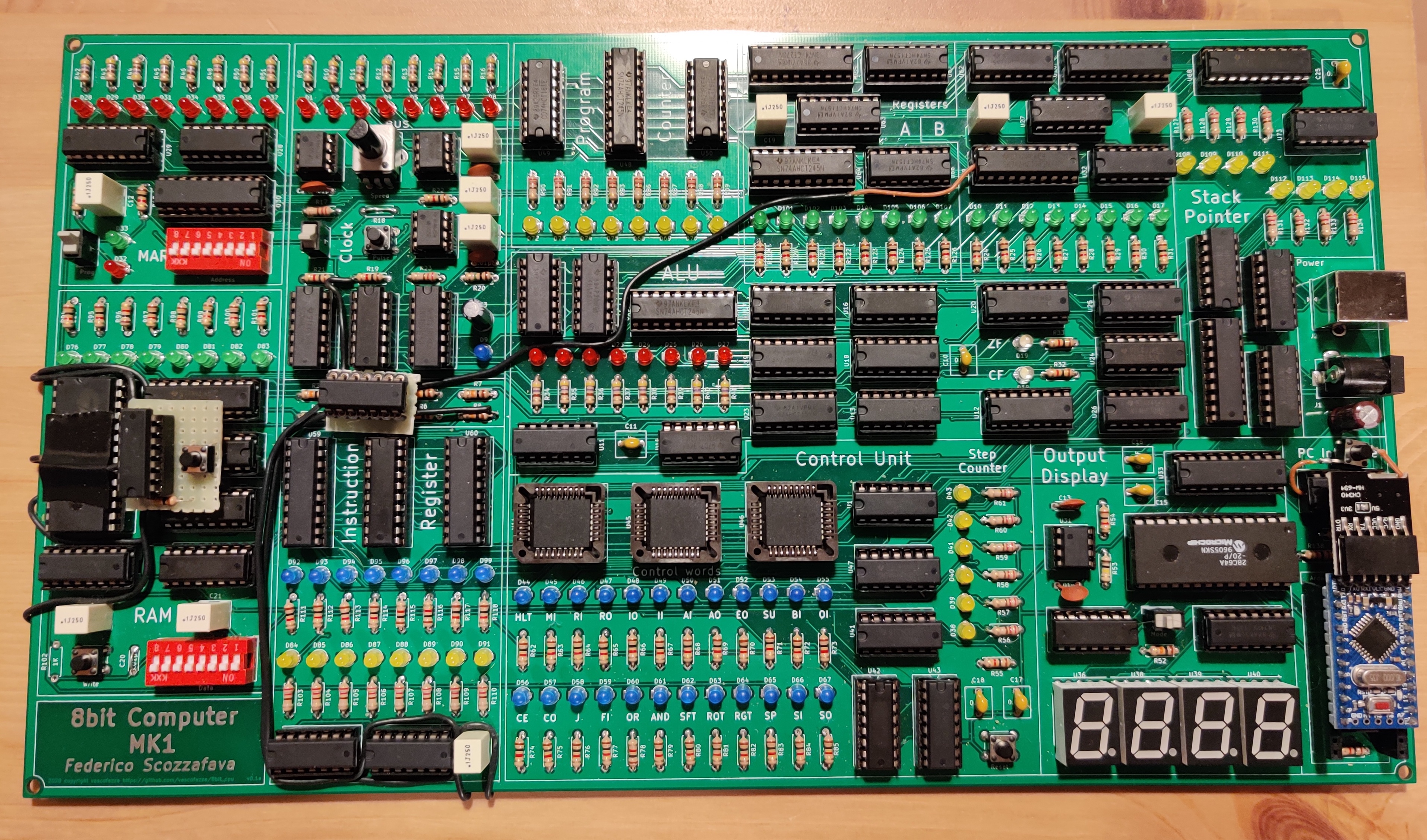
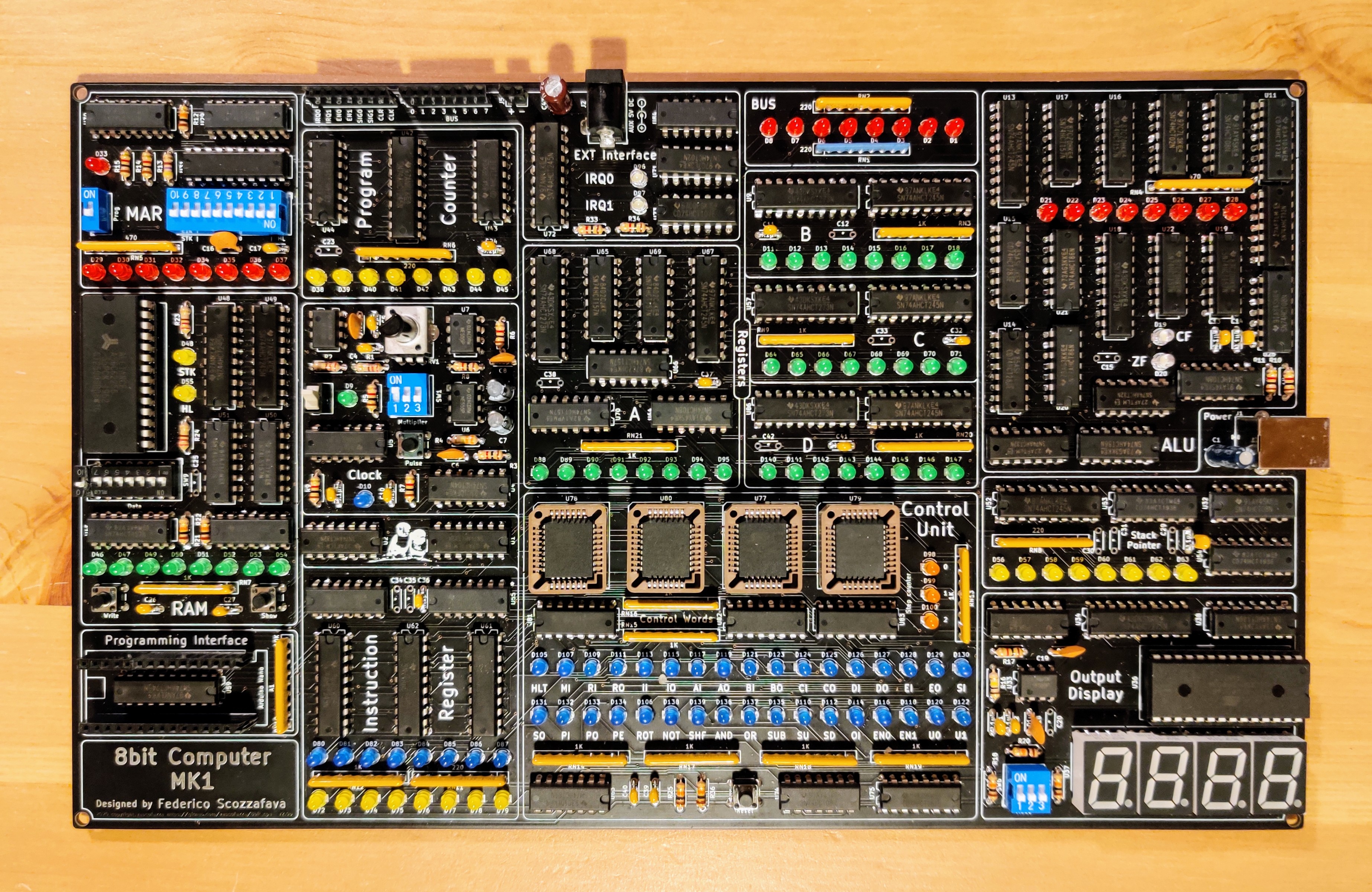
  • V 1.0 assembled:
  • V 2.0b assembled:
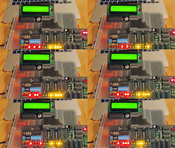
  • Helix Display Interface in action:
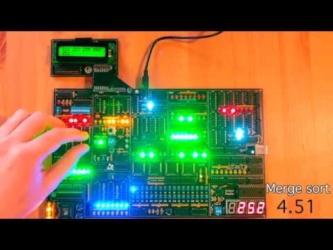
  • V 1.0 in action:

DEMO VIDEO (YouTube)

MK1 Computer - home-made Programmable 8bit CPU

Architecture

The MK1 CPU is composed of several modules, all connected trough a common 8-bit BUS, the status of each module is shown by dedicated LEDs.

  • The clock module is designed to allow step-by-step execution; in automatic mode the clock speed can be adjusted from 1Hz up to 32KHz.
  • The computer programs are stored in RAM and the CPU can be programmed both manually, by inserting binary machine code through dip-switches, and automatically via a USB PC interface.
    • The Programming interface is designed to be used in conjunction with an Arduino Nano or the Start9 programming board.
    • The Start9 programming board allows the loading of multiple programs stored on an on-board flash memory without the aid of an external computer device.
  • The Addressable memory space is 1024 byte, data, stack and code spaces are separated, the code address space is not writable.
  • The instructions are variable-length (see instruction-set here) 1 or 2 bytes long (first byte for the opcode, the second one for the argument), there are 4 general purpose registers (A, B, C, D) and a stack pointer register for subroutine calls.
  • The Arithmetic Logic Unit has a dedicated register for the second operand and supports the following operations:
    • Addition
    • Subtraction
    • OR
    • AND
    • NOT
    • Left/Right Shift
    • Left/Right Rotation
  • The Control Unit combinatory logic is implemented using EEPROMs (see microcode here) whilst each instruction is realized through a variable number of micro-instruction for a maximum of 6 micro-steps per instruction, including the fetch cycle. The instruction-set supports both direct and indirect memory access as well as absolute and conditional jumps on carry (CF) and zero (ZF) ALU flags.
  • The computation output can be visualized on a 4-digit display, with a dedicated register, able to represent positive and 2-complement negative numbers both in decimal and hexadecimal format.
  • The CPU can be extended thanks to the external BUS interface capable of handling up to 2 peripheral. The communication is bidirectional, the devices can send interrupts to the CPU to notify when new data is available. Interrupts are cleared once the data has been processed.
    • The only available peripheral at the moment is the Helix display interface, an ATmega328-driven 2x16 LCD output display.

Structure

  • MK1 CPU/:
    • 8bit-computer/: KiCad project, schematics and PCB design of the MK1 CPU.
    • code/:
      • microcode.py: generates the binary EEPROM microcode.
      • out_display.py: generates the binary output display EEPROM code.
      • uploader.py: uploads a binary MK1 program to the CPU.
      • mk1_computer_uploader/: Arduino programmer interface sketch.
    • assembler/: fork of the hlorenzi's assembler, improved and customized for the MK1
    • programs/: a collection of programs for the MK1 CPU plus the assembler definition
  • start9_programming_interface/:
    • programming_interface/: KiCad project, schematics and PCB design of the Start9 programming board.
    • code/start9_programming_interface/: Arduino code for the programming interface.
  • helix_display_interface/:
    • display_interface/: KiCad project, schematics and PCB design of the Helix display interface board.
    • code/helix_display_interface/: Arduino code for the display interface.
  • eeprom_programmer/: KiCad project, schematics and PCB design of a simple Arduino-based eeprom programmer
  • bus_breakout/: KiCad project, schematics and PCB design of the external bus connector breakout board.

Changelog

V2.0d:
  • minor hardware revision
  • revisited PCB design
  • new memory architecture, code memory section is read-only, stack and data live on separated spaces
V2.0b:
  • minor hardware revision
  • Variable-length instructions (1 or 2 bytes)
  • new custom assembler, thanks to https://github.com/hlorenzi/customasm
  • few new instructions
  • revisited microcode and instruction-set
V2.0:
  • 4 general purposes registers (A, B, C, D)
  • Stack Pointer implemented as an up-down counter
  • External interface and interrupt handling
  • Output display decodes HEX and ASCII values
  • Clock speed multipliers
  • Control Unit extended with 4 EEPROMs
  • Variable step microcode counter length (each instruction uses the minimum amount of micro-steps)
  • revisited microcode and instruction-set
V1.0:
  • Bugfixes.
  • HL and STK address signals available in the MAR dip-switch.
V0.1:
  • Initial release

Parts

16
QtyValueFootprintReferences
4MountingHole_2mmMountingHole:MountingHole_2mmM0, M1, M2, M3
2EXT BUSConnector_PinHeader_2.54mm:PinHeader_2x09_P2.54mm_VerticalJ3, J4
11ufCapacitor_THT:C_Disc_D4.3mm_W1.9mm_P5.00mmC1
1ATmega328-PUPackage_DIP:DIP-28_W7.62mm_SocketU1
1ContrastPotentiometer_THT:Potentiometer_Piher_PT-10-V10_VerticalRV1
1ContrastJumper:SolderJumper-3_P1.3mm_Bridged12_RoundedPad1.0x1.5mm_NumberLabelsJP1
1DisplayConnector_PinHeader_2.54mm:PinHeader_2x07_P2.54mm_VerticalJ1
1ENJumper:SolderJumper-3_P1.3mm_Open_RoundedPad1.0x1.5mm_NumberLabelsJP2
1IRQJumper:SolderJumper-3_P1.3mm_Open_RoundedPad1.0x1.5mm_NumberLabelsJP3
1LOGOSymbol:helix_smallS1
1LOGOSymbol:parrotS0
1ProgConnector_PinHeader_2.54mm:PinHeader_1x05_P2.54mm_VerticalJ2

Questions

How big is the Display interface PCB?

It measures 96.5 × 55.2 mm and has 2 copper layers, 1.6 mm thick.

What parts does the Display interface use?

16 parts, built around the ATMEGA328-PU. The full list of its parts is on this page, with links to each part's symbol and footprint where PCBKit's library has them.

Where can I download the Display interface KiCad files?

From the vascofazza/8bit-cpu repository on GitHub, at the commit this page was made from: the board is helix_display_interface/display_interface/display_interface.kicad_pcb. PCBKit opens the board in the browser, with nothing to install.

Can I use the Display interface design in my own project?

Its repository publishes it under the MIT licence: you may reuse it on that licence's terms (keep the author's notice, and for a copyleft licence share your changes alike).

More from vascofazza/8bit-cpu

4
  • 2 layers297.2 × 180.3 mm8bit computer, the printed circuit board in 3D

    8bit computer

    vascofazza/8bit-cpu

    Schematics & code for my 74LS-based 8-bit MK1 CPU

    377 parts317MIT
  • 2 layers53.3 × 48.3 mmProgramming interface, the printed circuit board in 3D

    Programming interface

    vascofazza/8bit-cpu

    Schematics & code for my 74LS-based 8-bit MK1 CPU

    15 parts317MIT
  • 2 layers68.7 × 53.5 mmArduino eeprom programmer, the printed circuit board in 3D

    Arduino eeprom programmer

    vascofazza/8bit-cpu

    Schematics & code for my 74LS-based 8-bit MK1 CPU

    9 parts317MIT
  • 2 layers57.1 × 41.9 mmBus breakout, the printed circuit board in 3D

    Bus breakout

    vascofazza/8bit-cpu

    Schematics & code for my 74LS-based 8-bit MK1 CPU

    4 parts317MIT

Similar boards

  • 2 layers104.9 × 75.2 mmHandipi kb, the printed circuit board in 3D

    Handipi kb

    brickbots/HandiPi

    Handheld RPI4 based computer with keyboard and display

    95 parts814MIT
  • 2 layers228 × 98 mmPlaid, the printed circuit board in 3D

    Plaid

    hsgw/plaid

    12x4 ortholinear usb keyboard made by Through Hole components ONLY.

    139 parts779MIT
  • 2 layers94.6 × 46.1 mmHeaterMeterPI, the printed circuit board in 3D

    HeaterMeterPI

    CapnBry/HeaterMeter

    HeaterMeter and LinkMeter Arduino BBQ Controller

    66 parts557MIT
  • 2 layers50 × 50 mmAvrcraft poed, the printed circuit board in 3D

    Avrcraft poed

    cnlohr/avrcraft

    Minecraft server optimized for 8-bit devices.

    58 parts471
  • 2 layers284.7 × 94.2 mmLumberjack, the printed circuit board in 3D

    Lumberjack

    peej/lumberjack-keyboard

    5x12 ortholinear through-hole component keyboard PCB for standard 60% cases

    165 parts403MIT
  • 2 layers132.1 × 45.7 mmIPoS, the printed circuit board in 3D

    IPoS

    peterheinrich/InternetOverSpaghetti

    Transmitting IP packages over a pair of spaghetti thus demonstrating how media independent IP really is.

    42 parts342
  • 2 layers63.3 × 57.2 mmRam Tester, the printed circuit board in 3D

    Ram Tester

    tops4u/Ram-Tester

    Ram Tester for vintage CBM Computer RAM Chips

    42 parts118
  • 2 layers285 × 117 mmTartan, the printed circuit board in 3D

    Tartan

    hsgw/tartan

    60% keyboard made by through-hole parts only

    171 parts98