2 layers45 × 100 mm
Walkiepcb
houseofthe051010/ESP32-Walkie-Talkie-V2
This ESP32 Walkie Talkie is redesigned with a SX1262 radio, a PCB, and a full case redesign.
93 parts1

 tyke01/bonk
An open source RC controller.
RC controller is an open-source printed circuit board by tyke01, from the tyke01/bonk repository on GitHub. It is a 4-layer board of 125 × 100 mm with 72 parts on 99 nets.
It is built around the ESP32-SL, COM-09032 and AP2112K-3.3, with the DW01A, TP4056-42-ESOP8 and USBLC6-2SC6 among its other parts. Its parts include 26 resistors, 17 capacitors, 10 ICs, 5 diodes and 5 switches. It belongs with the ESP32 boards of this library.


An open-source handheld RC transmitter built around the ESP32. Designed by Spectral Systems.
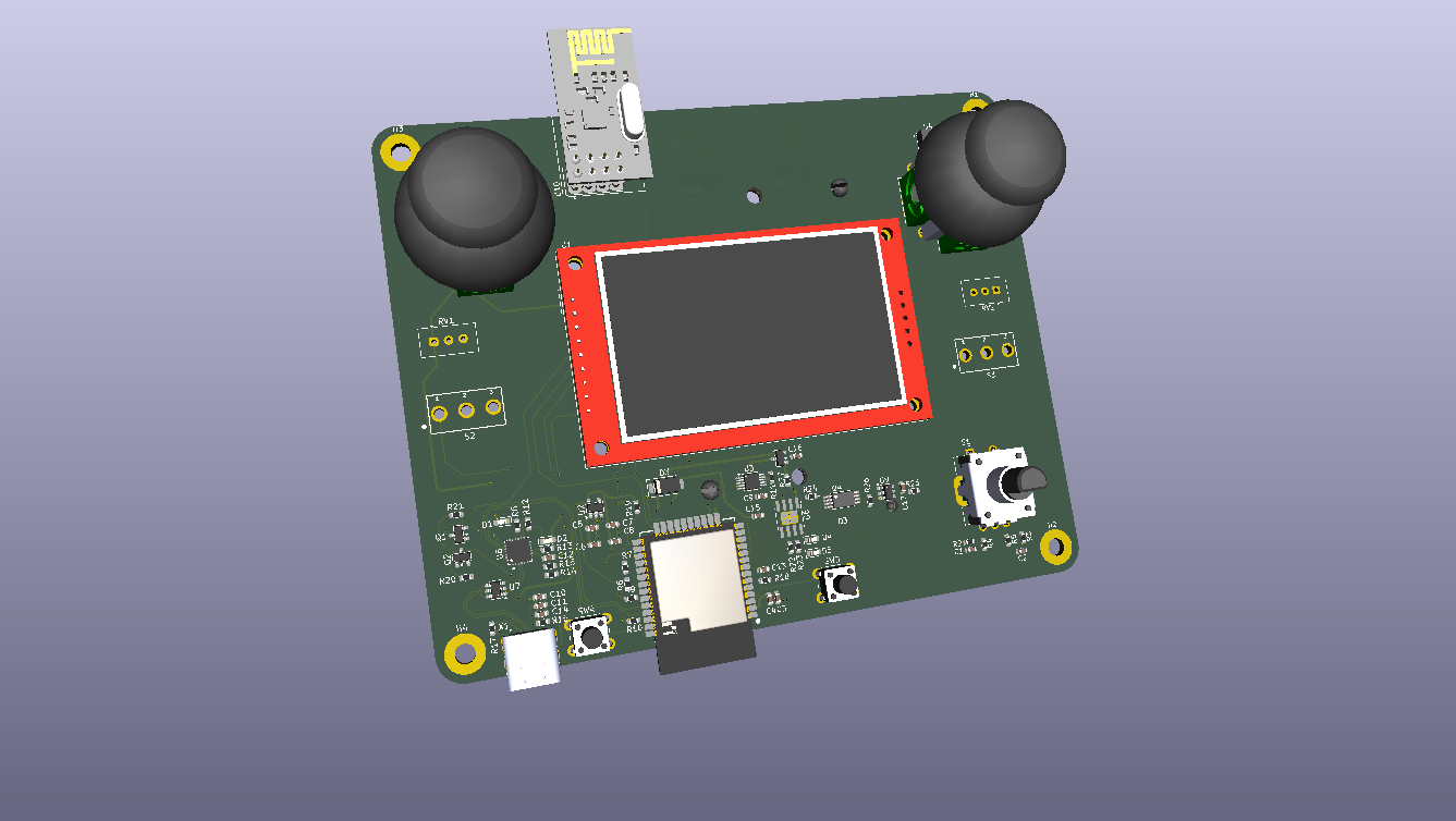
Status: Rev 1 (first PCB revision). The schematic passes ERC with 0 errors and the PCB passes DRC. Boards have been ordered but not yet assembled or tested, so expect errata. See Known issues before building one.
RC controller.kicad_pro     KiCad project
RC controller.kicad_sch     Schematic (single sheet, with design notes)
RC controller.kicad_pcb     PCB layout
RC controller.png           3D render
bom/
  ibom.html                 Interactive BOM (open in a browser for assembly)
  RC controller.csv         Raw BOM export
production/
  RC_controller.zip         Gerbers + drill files, ready to upload to JLCPCB
  bom.csv                   BOM for JLCPCB assembly
  positions.csv             Pick-and-place (CPL) file
  designators.csv
  netlist.ipc               IPC netlist (lets the fab run electrical tests)
placement/
  RC controller-all.pos     KiCad component placement file
Designed in KiCad 10.0.6. Open RC controller.kicad_pro to view everything.
| Block | Main parts | Notes |
|---|---|---|
| MCU | L1 ESP32-SL | Antenna overhangs the bottom board edge |
| USB-UART | U8 CP2102N (QFN-24), Q1/Q2 BC817 | DTR/RTS drive EN and IO0 for automatic bootloader entry |
| USB-C | X1 GCT USB4085-GF-A, U7 USBLC6-2SC6 | 5.1k pull-downs on CC1/CC2 (sink, default 5 V). USBLC6 provides ESD protection on D+/D- |
| Charger | U6 TP4056 (ESOP-8) | About 1.1 A charge current, set by R24 |
| Protection | U9 DW01A, Q4 FS8205A | Disconnects the cells on overcharge, overdischarge, or overcurrent |
| Load sharing | Q3 AO3401A, D3 SS34 | Runs the system from USB when plugged in, otherwise from the battery |
| Regulator | U2 AP2112K-3.3 | 600 mA LDO, single 3.3 V rail for everything |
| Battery monitor | U3 INA226, R11 20 mΩ | I2C address 0x40 |
| Display | U1 ILI9341 2.8" SPI module | Powered from 3.3 V |
| Radio | U10 nRF24L01 breakout | Shares the SPI bus with the display |
| Sticks | U4/U5 SparkFun COM-09032 | Powered from 3.3 V |
| Pots | RV1/RV2 | Powered from 3.3 V |
| Encoder | S1 Bourns PEC12R-4217F-S0024 | 10k pull-ups plus 10k/10 nF RC hardware debounce |
| Toggles | S2/S3 Würth 472123010111 | Switch to GND |
| Buttons | SW3 (EN/reset), SW4 (BOOT) | R18/C13 delay the release of EN at power-up |
| Battery holder | BT1 Keystone 1048 | 2x 18650, mounted on the bottom side |
| Net | What it is |
|---|---|
+5V | USB VBUS |
+VBAT_IN | Cell positive terminal |
BAT_P | Battery positive after the shunt. Charger output and Q3 drain connect here |
+VBAT_OUT | System rail (VSYS). Feeds the 3.3 V regulator |
+3V3 | Regulated 3.3 V for all logic |
BAT- | Raw cell negative |
GND | System ground (the switched negative, P-). Connected to BAT- through Q4 |
TP4056 BAT → BAT_P → R11 shunt → +VBAT_IN → cells → BAT- → Q4 (FS8205A) → GND → back to the TP4056
The return path goes through the protection MOSFETs. That's what allows the DW01A to stop charging if a cell reaches its overcharge limit.
+VBAT_OUT through D3 (about 4.5 V). Q3's gate sits at 5 V, so Q3 is off, and its body diode is reverse biased. The battery is isolated from the load and only the charger talks to it. Charge termination is therefore not confused by system current.+VBAT_OUT through Q3's low channel resistance. D3 blocks the battery from back-feeding the USB side.The DW01A watches the cell voltage and the voltage drop across the FS8205A. If it detects overcharge, overdischarge, or overcurrent, it turns off one of the two MOSFETs and disconnects BAT- from GND. R26 only feeds the DW01A's CS sense pin and carries no load current.
R11 (20 mΩ) is in series with the battery, so the INA226 sees both directions of current:
The full-scale range is about ±4 A (81.92 mV / 20 mΩ). The INA226's Vin+/Vin- traces are Kelvin-connected directly at R11's pads.
| GPIO | Module pin | Net | Function |
|---|---|---|---|
| 36 (SENSOR_VP) | 4 | JL_LR | Left stick X |
| 39 (SENSOR_VN) | 5 | JL_UD | Left stick Y (throttle) |
| 34 | 6 | JR_LR | Right stick X |
| 35 | 7 | JR_UD | Right stick Y |
| 32 | 8 | POT_L | Left potentiometer |
| 33 | 9 | POT_R | Right potentiometer |
| 25 | 10 | SW_L | Left toggle switch (to GND) |
| 26 | 11 | SW_R | Right toggle switch (to GND) |
| 27 | 12 | CLK | Encoder channel A |
| 14 | 13 | DT | Encoder channel B |
| 16 | 27 | SW | Encoder push switch (to GND) |
| 13 | 16 | LED | TFT backlight |
| 15 | 23 | CS | TFT chip select |
| 2 | 24 | DC | TFT data/command |
| 5 | 29 | CSN | nRF24 chip select |
| 4 | 26 | CE | nRF24 chip enable |
| 18 | 30 | SCK | SPI clock (through R7, 50 Ω) |
| 19 | 31 | MISO | SPI MISO (through R6, 50 Ω) |
| 23 | 37 | MOSI | SPI MOSI |
| 21 | 33 | SDA | I2C data |
| 22 | 36 | SCL | I2C clock |
| 1 (TXD0) | 35 | To CP2102N RXD | |
| 3 (RXD0) | 34 | From CP2102N TXD | |
| 0 | 25 | BOOT | BOOT button and auto-reset |
| EN | 3 | RST | Reset button, auto-reset, and TFT reset |
Unused: IO12 and IO17. The SD0 to SD3, CMD and CLK pins are reserved for the module's flash and must stay unconnected.
Why these pins:
| Device | Chip select | Other pins |
|---|---|---|
| ILI9341 TFT | IO15 (CS) | DC = IO2, reset = EN, backlight = IO13 |
| nRF24L01 | IO5 (CSN) | CE = IO4, IRQ not connected |
SCK = IO18, MOSI = IO23, MISO = IO19. Only one device is selected at a time.
| Device | Address | Pull-ups |
|---|---|---|
| INA226 | 0x40 (A0 = A1 = GND) | R9/R10, 4.7k to 3.3 V |
Firmware is developed separately with PlatformIO (Arduino framework). The following points are for anyone writing firmware for this board:
INPUT_PULLUP. A closed switch reads LOW.setRotation(3); check that this still fits the PCB orientation.LCSC numbers are the parts matched for the Rev 1 JLCPCB order. Stock and part numbers change, so verify each one before ordering. Full BOM files are in bom/ and production/.
| Designator | Value | Package | LCSC | Assembled by |
|---|---|---|---|---|
| C1, C2 | 10 nF 50 V X7R | 0603 | C57112 | JLC |
| C3, C5, C7, C9, C10, C14, C17 | 100 nF 50 V X7R | 0603 | C14663 | JLC |
| C11 | 4.7 µF 16 V X5R | 0603 | C19666 | JLC |
| C12, C13 | 1 µF 50 V X5R | 0603 | C15849 | JLC |
| C4, C6, C8, C15, C16 | 10 µF 10 V X5R | 0603 | C19702 | JLC |
| D1, D2, D4, D5 | LED, green | 0603 | C2289 (verify colour and Vf) | JLC |
| D3 | SS34 Schottky | SMA | C8678 | JLC |
| Q1, Q2 | BC817 NPN | SOT-23 | C22400355 | JLC |
| Q3 | AO3401A P-FET | SOT-23 | C15127 | JLC |
| Q4 | FS8205A dual N-FET | TSSOP-8 | Choose a TSSOP-8 variant (see Known issues) | JLC |
| R2-R5, R18-R21 | 10k 1% | 0603 | C25804 | JLC |
| R6, R7 | 50 Ω | 0603 | C849792 | JLC |
| R8, R12 | 470 Ω 1% | 0603 | C23179 | JLC |
| R9, R10 | 4.7k 1% | 0603 | C23162 | JLC |
| R11 | 20 mΩ 1% 1 W current sense | 1206 | C7420010 | JLC |
| R13, R22, R23, R26 | 1k 1% | 0603 | C21190 | JLC |
| R14 | 47.5k 1% | 0603 | C137715 | JLC |
| R15 | 22.1k 1% | 0603 | C2960862 | JLC |
| R16, R17 | 5.1k 1% | 0603 | C23186 | JLC |
| R24 | 1.1k 1% | 0603 | C54531154 | JLC |
| R25 | 100 Ω 1% | 0603 | C22775 | JLC |
| R27 | 100k 1% | 0603 | C25803 | JLC |
| U2 | AP2112K-3.3 | SOT-23-5 | C23380830 | JLC |
| U3 | INA226 | VSSOP-10 | C49851 | JLC |
| U6 | TP4056 | ESOP-8 | C16581 | JLC |
| U7 | USBLC6-2SC6 | SOT-23-6 | C2827654 | JLC |
| U8 | CP2102N-A02-GQFN24 | QFN-24 4x4 | C969151 | JLC |
| U9 | DW01A | SOT-23-6 | C351410 | JLC |
| L1 | ESP32-SL module | SMD module | C2764058 | Hand (was out of stock) |
| X1 | USB4085-GF-A USB-C | Through-hole | C7095263 | Hand |
| S1 | PEC12R-4217F-S0024 encoder | Through-hole | C49671241 | Hand |
| S2, S3 | 472123010111 toggle | Through-hole | C20040218 | Hand |
| U4, U5 | SparkFun COM-09032 joystick | Through-hole | C3283715 | Hand |
| RV1, RV2 | Potentiometer | Vishay T93YA footprint | Hand | |
| SW3, SW4 | Tactile switch 6 mm | Through-hole | Hand | |
| U1 | 2.8" ILI9341 SPI TFT module | Header | Hand | |
| U10 | nRF24L01 breakout | 2x4 header | Hand | |
| BT1 | Keystone 1048 2x 18650 holder | SMD, bottom side | Hand |
Fabricated at JLCPCB. Upload production/RC_controller.zip.
| Setting | Value |
|---|---|
| Layers | 4 |
| Size | 125 x 100 mm |
| Thickness | 1.6 mm |
| Outer copper | 1 oz |
| Surface finish | HASL works for hand soldering. ENIG is better for the 0.5 mm pitch parts (U3, U8) |
Stackup:
| Layer | Use |
|---|---|
| F.Cu | Signals and components, with GND pour |
| In1.Cu | Solid GND plane |
| In2.Cu | GND plane |
| B.Cu | Signals, plus the battery holder |
Design rules used: 0.2 mm default tracks and clearance, 0.5 mm power tracks, 1.0 mm battery tracks, 0.6/0.3 mm vias. USB D+/D- are routed as a differential pair over the In1 GND plane. There is a copper keepout under the ESP32 antenna on all layers.
Notes:
The Rev 1 order uses JLCPCB partial assembly: JLC places the SMT parts on the top side, and the rest is hand-soldered.
Before ordering assembly:
Hand-soldering order (suggested):
The interactive BOM (bom/ibom.html) highlights where each part goes.
Work through this in order, and don't insert the cells until step 4.
+5V, +VBAT_OUT, +3V3 and BAT_P. None of them should read close to 0 Ω.+5V ≈ 5 V+VBAT_OUT ≈ 4.5 V (5 V minus the SS34 drop)+3V3 ≈ 3.3 VThe hardware design files are licensed under the CERN Open Hardware Licence Version 2, Permissive (CERN-OHL-P-2.0). See the LICENSE file.
Under this licence you may use, study, modify, make and sell the design, as long as you keep the copyright and licence notices. Firmware, once published, will be licensed separately.
Designed by Victor Macharia (Syb0rg), Spectral Systems. Repository: github.com/tyke01/bonk
Contributions, issue reports, and build photos are welcome. Please open an issue if you build one.
| Qty | Value | Footprint | References |
|---|---|---|---|
| 8 | 10K | Resistor_SMD:R_0603_1608Metric | R2, R3, R4, R5, R18, R19, R20, R21 |
| 7 | 0.1u | Capacitor_SMD:C_0603_1608Metric | C3, C5, C7, C9, C10, C14, C17 |
| 5 | 10u | Capacitor_SMD:C_0603_1608Metric | C4, C6, C8, C15, C16 |
| 4 | 1k | Resistor_SMD:R_0603_1608Metric | R13, R22, R23, R26 |
| 4 | LED | LED_SMD:LED_0603_1608Metric_Pad1.05x0.95mm_HandSolder | D1, D2, D4, D5 |
| 2 | 10nf | Capacitor_SMD:C_0603_1608Metric | C1, C2 |
| 2 | 1u | Capacitor_SMD:C_0603_1608Metric | C12, C13 |
| 2 | 470 | Resistor_SMD:R_0603_1608Metric | R8, R12 |
| 2 | 472123010111 | toggle_switch:toggle_switch | S2, S3 |
| 2 | 4k7 | Resistor_SMD:R_0603_1608Metric | R9, R10 |
| 2 | 50 | Resistor_SMD:R_0603_1608Metric | R6, R7 |
| 2 | 5k1 | Resistor_SMD:R_0603_1608Metric | R16, R17 |
| 2 | BC817 | Package_TO_SOT_SMD:SOT-23 | Q1, Q2 |
| 2 | COM-09032 | XDCR_COM-09032:XDCR_COM-09032 | U4, U5 |
| 2 | R_Potentiometer | Potentiometer_THT:Potentiometer_Vishay_T93YA_Vertical | RV1, RV2 |
| 2 | SW_Push | Button_Switch_THT:SW_PUSH_6mm_H7.3mm | SW3, SW4 |
| 1 | 100 | Resistor_SMD:R_0603_1608Metric | R25 |
| 1 | 100k | Resistor_SMD:R_0603_1608Metric | R27 |
| 1 | 1048 | Battery_Holder_18650_2_Cell_SMD:Battery_Holder_18650_2_Cell_SMD | BT1 |
| 1 | 1k1 | Resistor_SMD:R_0603_1608Metric | R24 |
| 1 | 20m | Resistor_SMD:R_0603_1608Metric | R11 |
| 1 | 22k1 | Resistor_SMD:R_0603_1608Metric | R15 |
| 1 | 4.7u | Capacitor_SMD:C_0603_1608Metric | C11 |
| 1 | 47k5 | Resistor_SMD:R_0603_1608Metric | R14 |
| 1 | AO3401A | Package_TO_SOT_SMD:SOT-23 | Q3 |
| 1 | AP2112K-3.3 | Package_TO_SOT_SMD:SOT-23-5 | U2 |
| 1 | CP2102N-Axx-xQFN24 | Package_DFN_QFN:QFN-24-1EP_4x4mm_P0.5mm_EP2.6x2.6mm | U8 |
| 1 | CR2013-MI2120 | Display:CR2013-MI2120 | U1 |
| 1 | DW01A | Package_TO_SOT_SMD:SOT-23-6 | U9 |
| 1 | ESP32-SL | WIFIM-SMD_ESP32-SL:WIFIM-SMD_ESP32-SL | L1 |
| 1 | FS8205A | SOP65P640X120-8N:SOP65P640X120-8N | Q4 |
| 1 | INA226 | Package_SO:TSSOP-10_3x3mm_P0.5mm | U3 |
| 1 | NRF24L01_Breakout | RF_Module:nRF24L01_Breakout | U10 |
| 1 | PEC12R-4217F-S0024 | XDCR_PEC12R-4217F-S0024:XDCR_PEC12R-4217F-S0024 | S1 |
| 1 | SS34 | Diode_SMD:D_SMA | D3 |
| 1 | TP4056-42-ESOP8 | Package_SO:SOIC-8-1EP_3.9x4.9mm_P1.27mm_EP2.41x3.3mm_ThermalVias | U6 |
| 1 | USB4085-GF-A | USB4085_CONNECTOR:USB4085_CONNECTOR | X1 |
| 1 | USBLC6-2SC6 | Package_TO_SOT_SMD:SOT-23-6 | U7 |
It measures 125 × 100 mm and has 4 copper layers, 1.6 mm thick.
72 parts, built around the ESP32-SL, COM-09032, AP2112K-3.3 and DW01A. The full list of its parts is on this page, with links to each part's symbol and footprint where PCBKit's library has them.
From the tyke01/bonk repository on GitHub, at the commit this page was made from: the board is _restore_backup_2026-09-24T16-39-22-534/RC controller.kicad_pcb and its schematic RC controller.kicad_sch. PCBKit opens the board in the browser, with nothing to install.
Its repository states no licence, so its author keeps all rights: ask tyke01 before reusing the design.
houseofthe051010/ESP32-Walkie-Talkie-V2
This ESP32 Walkie Talkie is redesigned with a SX1262 radio, a PCB, and a full case redesign.


g210101021/OpenStylophone-RP2040
Overview • Technical Summary • Architecture • Hardware Audit & Remediation • Schematic Subsystems • PCB Layout • Firmware Roadmap • Bill of Materials • Author

jonny190/TableLight
A 3D-printable, battery-powered, USB-C rechargeable table lamp in the classic "Poldina" shape - honeycomb disc base, thin stem, down-firing cone shade with a white top - running WLED on an ESP32, with a capacitive touch…


