
4 layers99 × 53.3 mm
PSLab
fossasia/pslab-hardware
PSLab Hardware Design and Schematics https://pslab.io
199 parts1.7kApache-2.0

 tomatoesong/HE_Leverless
Hall effect sensor based 13 key leverless fight pad controller
HE Leverless Mainboard is an open-source printed circuit board by tomatoesong, from the tomatoesong/HE_Leverless repository on GitHub, published under the MIT licence. It is a 2-layer board of 270 × 138 mm with 62 parts on 47 nets, routed with 418 tracks and 82 vias.
It is built around the WS2812B. Its parts include 21 capacitors and 8 diodes. It belongs with the sensors and measurement and computers and single-board computers boards of this library.
A custom-built fighting game controller featuring Hall effect sensors based on ESP32-S3 for ultra-durable, low latency performance. Designed for competitive play, modularity, and long-term reliability.
| Front View |
|---|
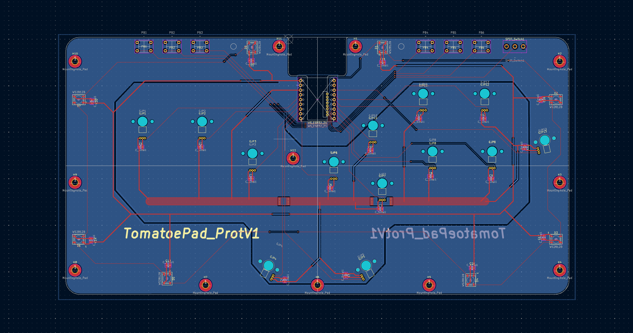 |
Created Using KiCad and custom library and footprints!
| Startup View | Selection | Save with Ease |
|---|---|---|
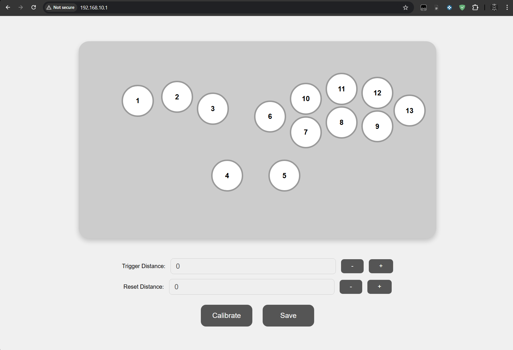 | 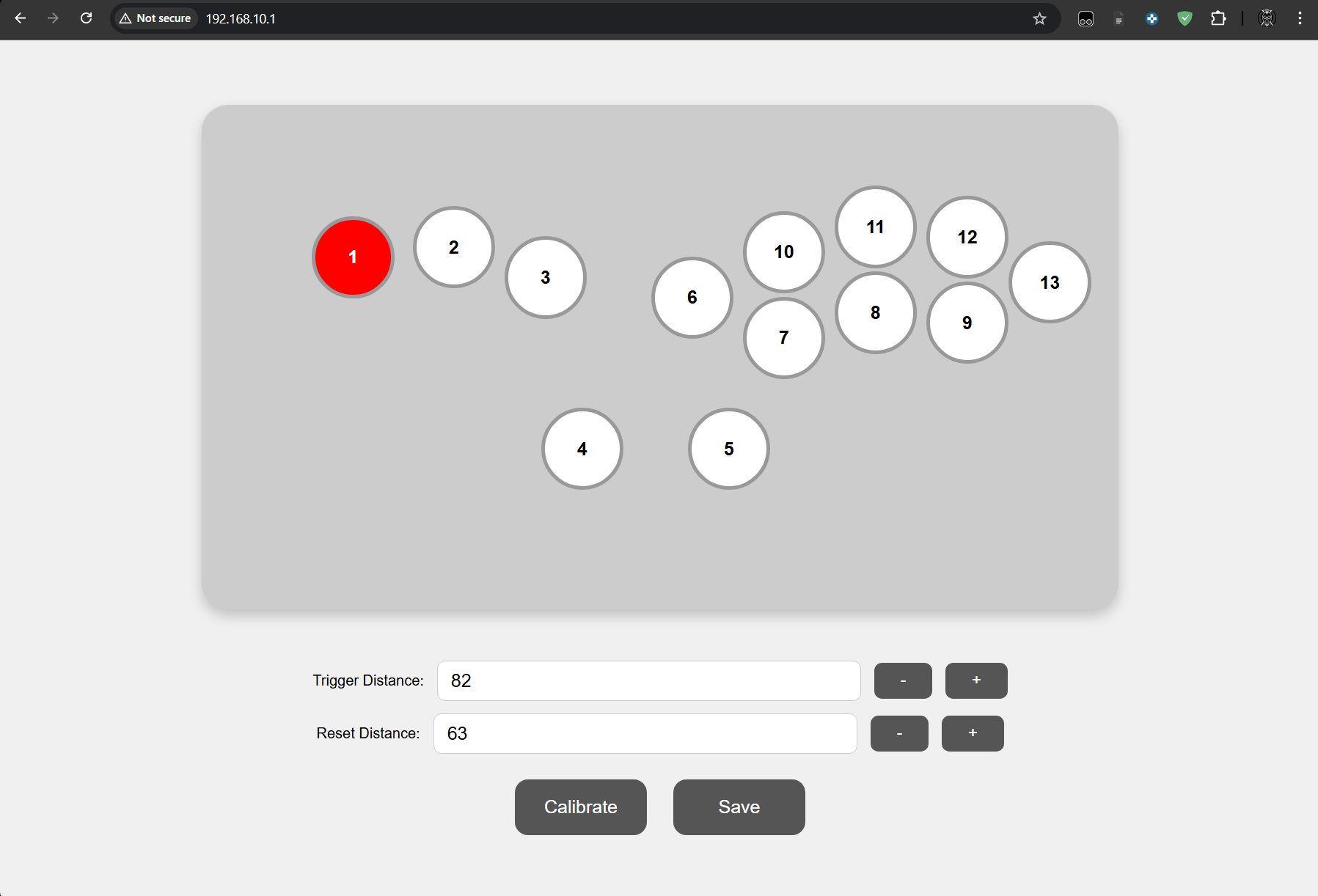 | 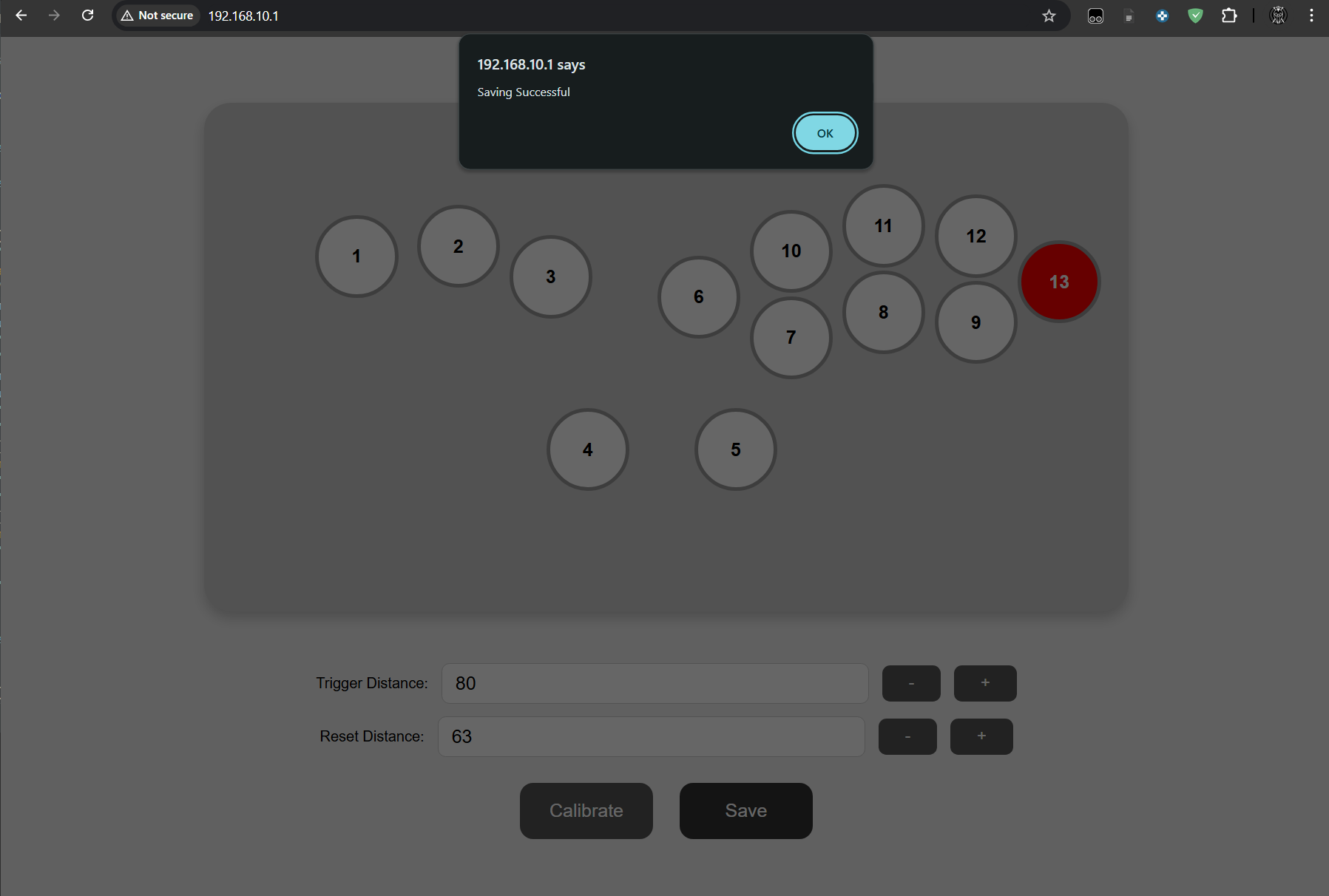 |
Fully integrated and interactable WEB UI from an embedded board
| Front View |
|---|
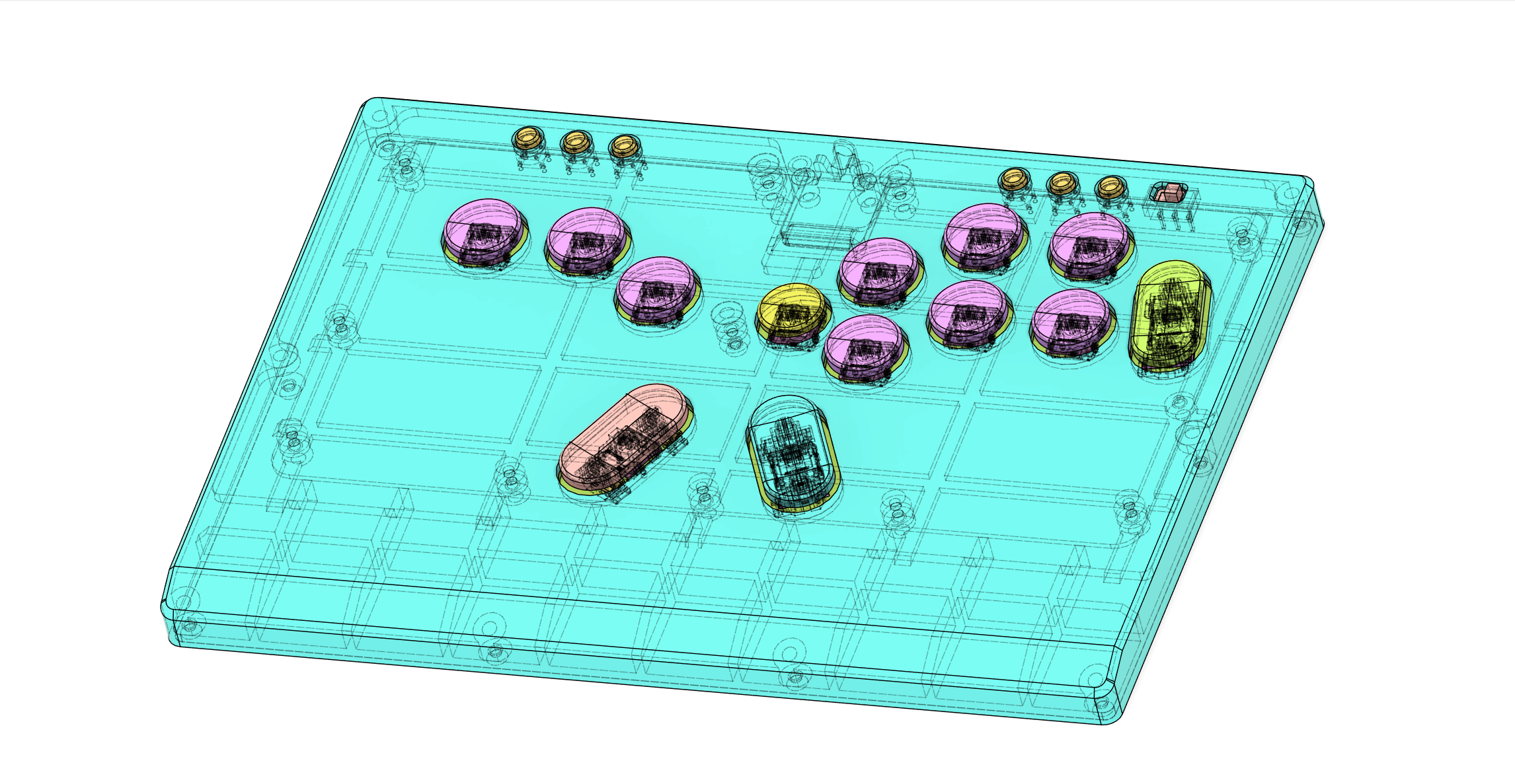 |
| WireFrame View |
|---|
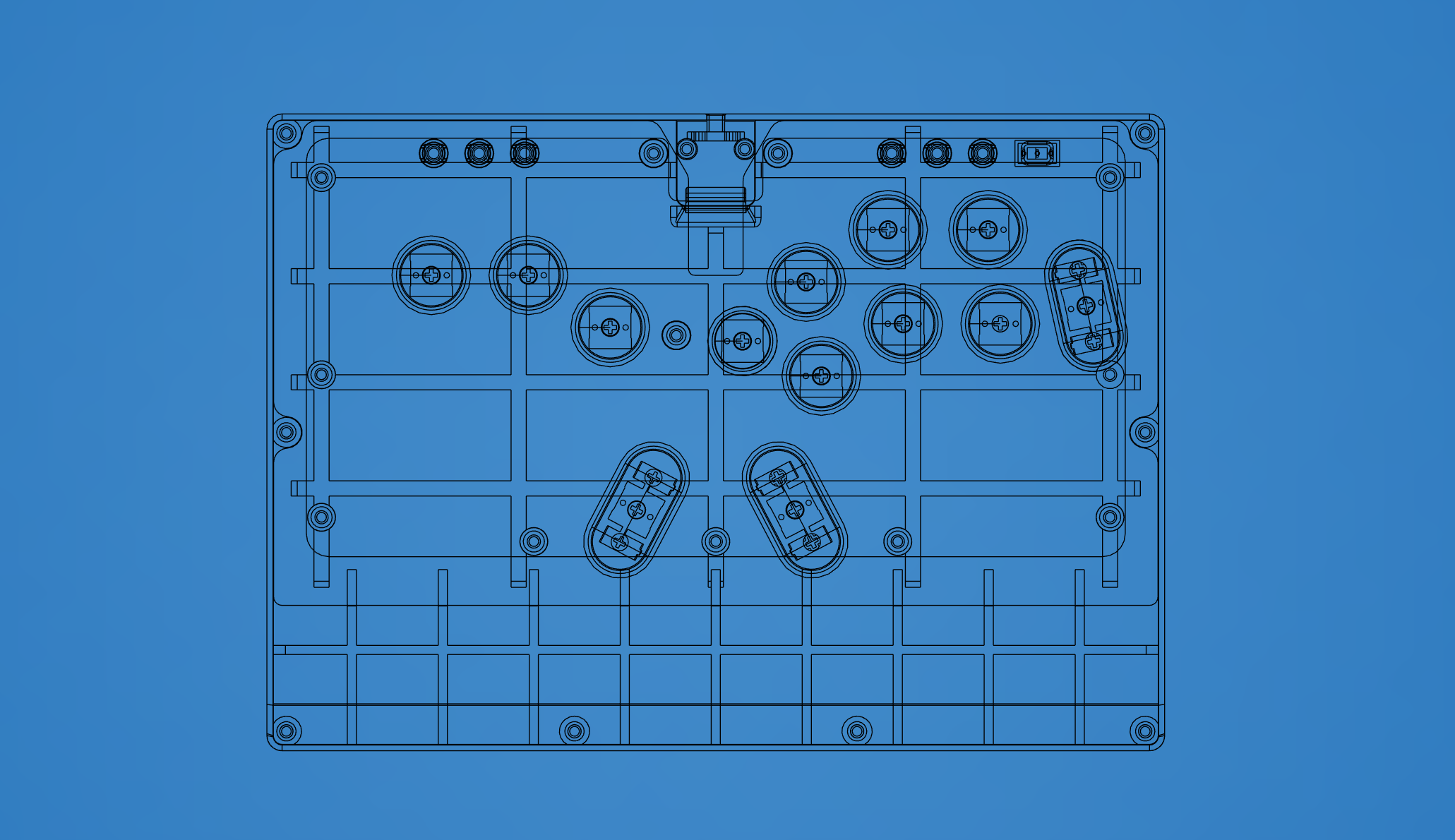 |
Designed in Fusion360 with all components modeled for accuracy.
git clone https://github.com/your-username/your-controller-repo.git| Qty | Value | Footprint | References |
|---|---|---|---|
| 21 | C_Small | Capacitor_SMD:C_0805_2012Metric | C1, C2, C3, C4, C10, C11, C12, C13, C14, C15, C16, C17, C18, C19, C20, C21 +5 |
| 12 | MountingHole_Pad | MountingHole:MountingHole_3.2mm_M3_Pad | H1, H2, H3, H4, H5, H6, H7, H8, H9, H10, H11, H12 |
| 10 | ~ | HE_Leverless_Library:Gateron_Jade_Pro | GJP1, GJP2, GJP3, GJP6, GJP7, GJP8, GJP9, GJP10, GJP11, GJP12 |
| 8 | WS2812B | LED_SMD:LED_WS2812B_PLCC4_5.0x5.0mm_P3.2mm | D1, D2, D3, D4, D5, D6, D7, D8 |
| 6 | ~ | HE_Leverless_Library:6x6_PushButton | PB1, PB2, PB3, PB4, PB5, PB6 |
| 2 | ~ | HE_Leverless_Library:Gateron_Jade_Pro_2 | GJP5, GJP13 |
| 1 | ~ | HE_Leverless_Library:Gateron_Jade_Pro_3 | GJP4 |
| 1 | ~ | HE_Leverless_Library:WS_ESP32_S3_Zero | WS_ESP32_Z1 |
| 1 | ~ | HE_Leverless_Library:1P2T_SPDT_Switch | SPDT_Switch1 |
fossasia/pslab-hardware
PSLab Hardware Design and Schematics https://pslab.io

FrameworkComputer/ExpansionCards
Reference designs and documentation to create Expansion Cards for the Framework Laptop


PrintersForAnts/Micron
If you want to purchase full kits there are 3 available (Kits are slowly updating to R1 hardware just make sure to double check the included hardware in your kit and if you have any questions reach out in the discord)


It measures 270 × 138 mm and has 2 copper layers, 1.6 mm thick.
62 parts, built around the WS2812B. The full list of its parts is on this page, with links to each part's symbol and footprint where PCBKit's library has them.
From the tomatoesong/HE_Leverless repository on GitHub, at the commit this page was made from: the board is HE_Leverless_Mainboard/HE_Leverless_Mainboard.kicad_pcb and its schematic HE_Leverless_MB_V2/HE_Leverless_MB_V2.kicad_sch. PCBKit opens the board in the browser, with nothing to install.
Its repository publishes it under the MIT licence: you may reuse it on that licence's terms (keep the author's notice, and for a copyleft licence share your changes alike).