2 layers99.8 × 50.1 mm
 tinkermax/split-flap13
DIY mechanical spli-flap display
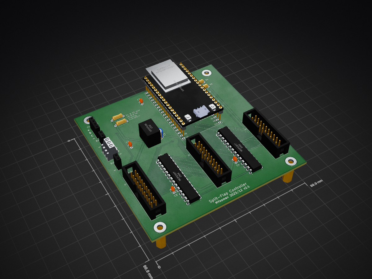
Split flap is an open-source printed circuit board by tinkermax, from the tinkermax/split-flap repository on GitHub, published under the CC-BY-4.0 licence. It is a 2-layer board of 99.9 × 99.9 mm with 28 parts on 76 nets, routed with 474 tracks and 30 vias.
It is built around the ESP32-DEVKITC-VE, MCP23017-E/SP and LD1117V33. Its parts include 7 connectors, 5 capacitors, 4 resistors and 4 ICs. It belongs with the lEDs and displays boards and the ESP32 boards of this library.


You can find full details and discussion on my blog.

This is an alternate electronics and firmware for David Kingsman's Split-Flap Display.
DEBUG 1
unitCount 12
NETWORKNAME "splitflap"
calOffsetUnit : an array of the offsets to move from hall sensor trigger to blank flap
FlapStep : an array containing the number of steps per stepper revolution (then divided by 45 flaps)
WIFI_SSID "mySSID"
WIFI_PWD "myPassword"
MY_NTP_SERVER "au.pool.ntp.org" // Set the best fitting NTP server (pool) for your location
MY_TZ "AEST-10AEDT,M10.1.0,M4.1.0/3" // Set your time zone from https://github.com/nayarsystems/posix_tz_db/blob/master/zones.csv
WORDNIKAPIKEY "" // Get your private key from https://developer.wordnik.com/
MINWORDLEN 9 // Specify minimum word length to fetch from Wordnik
WORDUPDATESPERHOUR 1 // Set number of word updates from https://wordnik.com per hour. 0 will disable, else use an integer that results in an exact number of minutes btw updates i.e. 1,2,3,4,5,6,10,12,15,20,30 or 60
This project makes extensive use of two libraries:
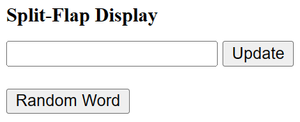
{
    displaytext: "Display Text"
}
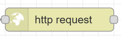
For example, you could use the request node within node-red:

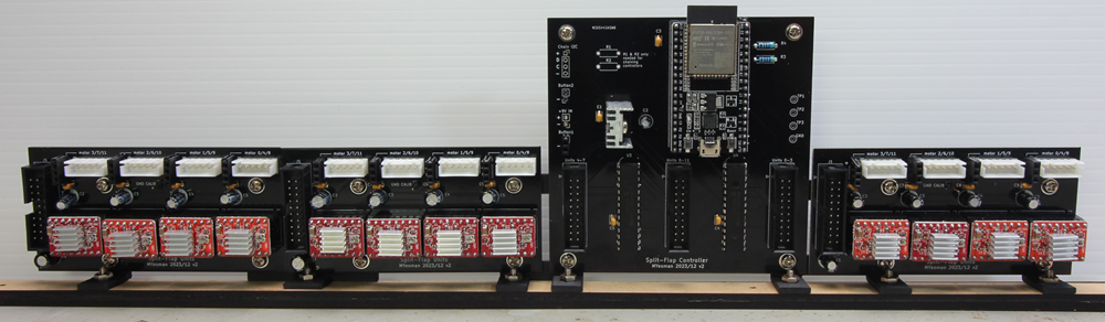
Schematics for the Controller and Unit PCBs can be found under schematics.
Gerbers, Bill of materials and Kicad source files can be found under PCBs.
PCB mounting brackets can be found on Printables.
Also found there is my remixed unit frame. This is optional, as you could still use the original frames with the new electronics.
My unit frame requires an additional two M3*L3*D4 heat inserts for connecting to the adjacent unit.
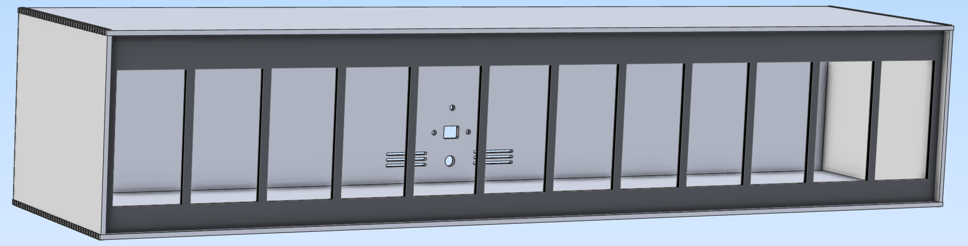
front
rear
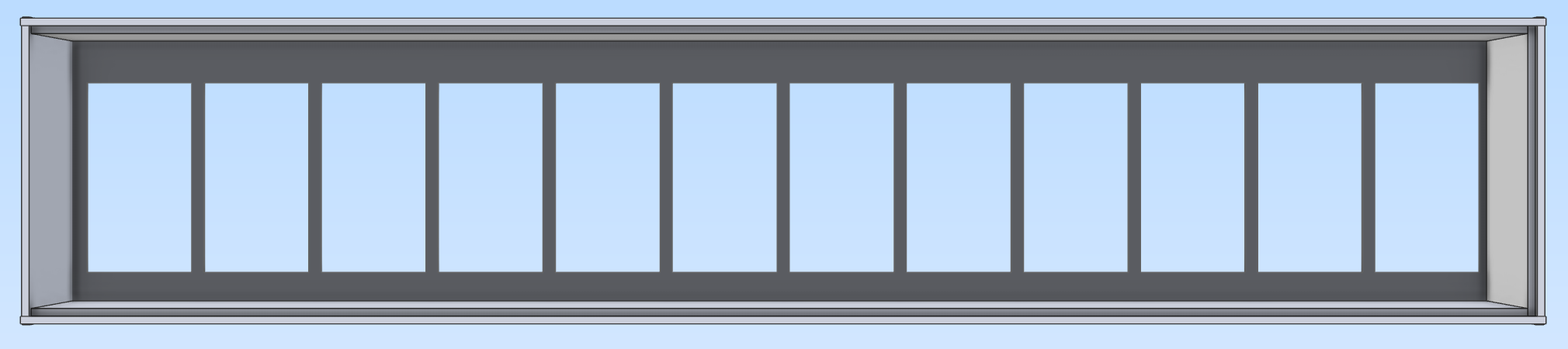
Plywood (3mm) files for laser cutting are in enclosure
Copyright (c) 2024 Malcolm Yeoman.
Electronics is released under CERN-OHL-P (Permissive) V2.
Firmware is released under the MIT License.
Documentation is licensed under a Creative Commons Attribution 4.0 International License.
| Qty | Value | Footprint | References |
|---|---|---|---|
| 4 | 100nF | Capacitor_THT:C_Disc_D3.4mm_W2.1mm_P2.50mm | C1, C3, C4, C5 |
| 4 | 4K7 | Resistor_THT:R_Axial_DIN0207_L6.3mm_D2.5mm_P7.62mm_Horizontal | R1, R2, R3, R4 |
| 4 | 5000 | digikey-footprints:Test_Point_D1.02mm | TP1, TP2, TP3, TP4 |
| 4 | MountingHole_3.2mm_M3_Pad | MountingHole:MountingHole_3.2mm_M3_Pad | REF1, REF2, REF3, REF4 |
| 2 | MCP23017 | digikey-footprints:DIP-28_W7.62mm | U3, U4 |
| 1 | +9V IN | TerminalBlock_TE-Connectivity:TerminalBlock_TE_282834-3_1x03_P2.54mm_Horizontal | J1 |
| 1 | 10uF | Capacitor_THT:CP_Radial_D5.0mm_P2.00mm | C2 |
| 1 | Button1 | Connector_PinSocket_2.54mm:PinSocket_1x02_P2.54mm_Vertical | J3 |
| 1 | Button2 | Connector_PinSocket_2.54mm:PinSocket_1x02_P2.54mm_Vertical | J4 |
| 1 | Chain I2C | Connector_PinSocket_2.54mm:PinSocket_1x04_P2.54mm_Vertical | J2 |
| 1 | ESP32-DevKitC | PCM_Espressif:ESP32-DevKitC | U2 |
| 1 | LD1117V33 | digikey-footprints:TO-220-3 | U1 |
| 1 | Units 0-3 | Connector_IDC:IDC-Header_2x10_P2.54mm_Vertical | J5 |
| 1 | Units 4-7 | Connector_IDC:IDC-Header_2x10_P2.54mm_Vertical | J6 |
| 1 | Units 8-11 | Connector_IDC:IDC-Header_2x10_P2.54mm_Vertical | J7 |
It measures 99.9 × 99.9 mm and has 2 copper layers, 1.6 mm thick.
28 parts, built around the ESP32-DEVKITC-VE, MCP23017-E/SP and LD1117V33. The full list of its parts is on this page, with links to each part's symbol and footprint where PCBKit's library has them.
From the tinkermax/split-flap repository on GitHub, at the commit this page was made from: the board is PCBs/Kicad/Controller/split-flap.kicad_pcb and its schematic PCBs/Kicad/Controller/split-flap.kicad_sch. PCBKit opens the board in the browser, with nothing to install.
Its repository publishes it under the CC-BY-4.0 licence: you may reuse it on that licence's terms (keep the author's notice, and for a copyleft licence share your changes alike).

rimuadmin/TeensyMaestro-Hardware
Hardware for the TeensyMaestro

Alli-Ekundayo/scpt-rl
SCPT-RL trains a cross-attention transformer policy to place PCB components sequentially on a discrete grid. Training has two phases:

arthurkowskii/AKOR_01
having fun building a synth ! C++ programming, PCB design with KiCad, and hands-on hardware work in what some people call “the real world.”


Kalilinuxloverr/Desk-Mate
Wall-E-artiger Schreibtisch-Begleiter: Ampel fuer Claude Code & Downloads, Motorfader, Augen-Displays. ESP32-S3, Swift, KiCad, 3D-Druck.


OverInvented/Flippy
The code needed to build a mechanical 7-segment display that uses electromagnets to display characters
