2 layers29 × 40 mm
ESP8266-12 breakout
timelab/ADEM
Mobile device for distributed measurements of particulate matter (fine dust)
19 parts13LGPL-3.0
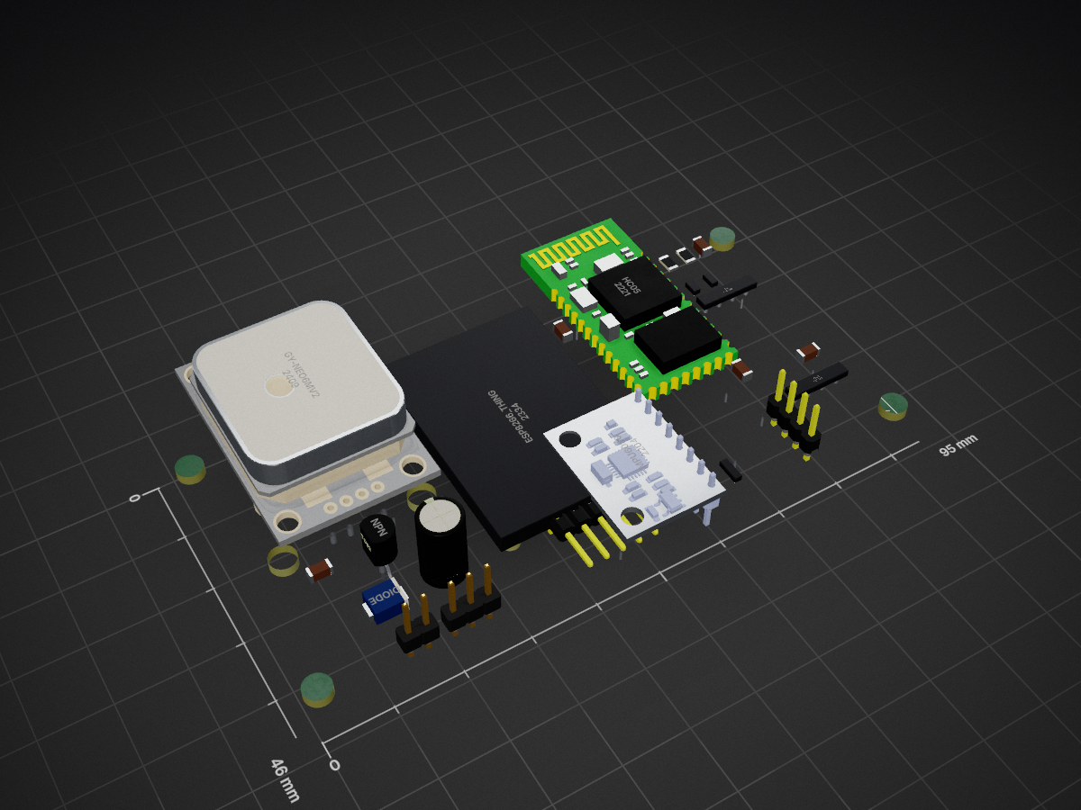
 timelab/ADEM13
Mobile device for distributed measurements of particulate matter (fine dust)
ADEM is an open-source printed circuit board by timelab, from the timelab/ADEM repository on GitHub, published under the LGPL-3.0 licence. It is a 2-layer board of 93 × 42 mm with 29 parts on 33 nets, routed with 328 tracks and 21 vias.
It is built around the BMP180 and HTU21D. Its parts include 7 capacitors, 7 ICs, 3 resistors, 3 connectors and 1 diode. It belongs with the sensors and measurement boards and the ESP8266 boards of this library.


| Qty | Value | Footprint | References |
|---|---|---|---|
| 6 | C | Capacitors_SMD:C_1206_HandSoldering | C1, C2, C3, C4, C5, C6 |
| 3 | R | Resistors_SMD:R_1206_HandSoldering | R1, R2, R3 |
| 2 | GS_A0 | Connect:GS3 | GS_MPU1, GS_NV1 |
| 1 | BMP180 | ADEM:BMP180 | U6 |
| 1 | CONN_01X03 | Connect:PINHEAD1-3 | P2 |
| 1 | CONN_01X04 | Pin_Headers:Pin_Header_Straight_1x04 | P3 |
| 1 | CONN_01X05 | Pin_Headers:Pin_Header_Angled_1x05 | P_SENS1 |
| 1 | CONN_buzz | Connect:PINHEAD1-2 | P1 |
| 1 | CP | Capacitors_Elko_ThroughHole:Elko_vert_11.2x6.3mm_RM2.5 | C7 |
| 1 | DIODE | Diodes_SMD:SMB_Handsoldering | D1 |
| 1 | ESP8266_THING | ADEM:ESP8266_THING | U3 |
| 1 | GS1 | Connect:GS2 | GS1 |
| 1 | GS2 | Connect:GS2 | GS2 |
| 1 | GS_A1 | Connect:GS3 | GS_NV2 |
| 1 | GS_A2 | Connect:GS3 | GS_NV3 |
| 1 | GY-NEO6MV2 | ADEM:GY-NEO6MV2 | U1 |
| 1 | HC05 | ADEM:HC-05 | U2 |
| 1 | HTU21D | ADEM:HTU21D | U7 |
| 1 | MPU6050 | ADEM:MPU6050 | U4 |
| 1 | NPN | TO_SOT_Packages_THT:TO-92_Inline_Wide | Q1 |
| 1 | NVSRAM | Housings_SOIC:SOIC-8_3.9x4.9mm_Pitch1.27mm | U5 |
timelab/ADEM
Mobile device for distributed measurements of particulate matter (fine dust)

jrleeman/WxBackpack
Backpack board for the Light Blue Bean containing weather sensors.


ldab/Node-RED-Energy-Harvesting-dashboard
Node-RED Energy Harvesting dashboard example, weather forecast, temperature and humidty measurement. MQTT, ESP32, u-blox NINA-W10, HTU21D, IBM Cloud, CloudMQTT

VitalSeptfonds/OpenWeatherStation
Open Wheather Station based on STM32


dimhoff/sensof
Si4010 based wireless sensors(temperature, humidity, etc.) firmware and utilities


zegarac/Photosynq-hardware
Photosynq KiCad files for the main board and other associated hardware
It measures 93 × 42 mm and has 2 copper layers, 1.6 mm thick.
29 parts, built around the BMP180 and HTU21D. The full list of its parts is on this page, with links to each part's symbol and footprint where PCBKit's library has them.
From the timelab/ADEM repository on GitHub, at the commit this page was made from: the board is docs/kicad/ADEM/ADEM.kicad_pcb. PCBKit opens the board in the browser, with nothing to install.
Its repository publishes it under the LGPL-3.0 licence: you may reuse it on that licence's terms (keep the author's notice, and for a copyleft licence share your changes alike).