2 layers209.8 × 147 mm
Kicad miao panel
kilipan/miao
A cheap and hand-solderable drop-in replacement for the XIAO using ch552t
2,645 parts33CERN-OHL-S-2.0

 ThePurox/Hexapoda13
The electronic design is inspired by the MIAO MCU board.
Butterfly is an open-source printed circuit board by ThePurox, from the ThePurox/Hexapoda repository on GitHub. It is a 2-layer board of 193.5 × 116.6 mm with 67 parts on 59 nets, routed with 693 tracks and 255 vias.
It is built around the USBLC6-2SC6, BAV70 and PMEG2010EA. Its parts include 32 switches, 16 diodes, 3 resistors, 2 capacitors and 2 ICs.


The Hexapoda is a hummingbird style 30 key keyboard designed around hexagonal keycaps, which require Choc v1 switches.
It uses the CH552T controller and FAK firmware.
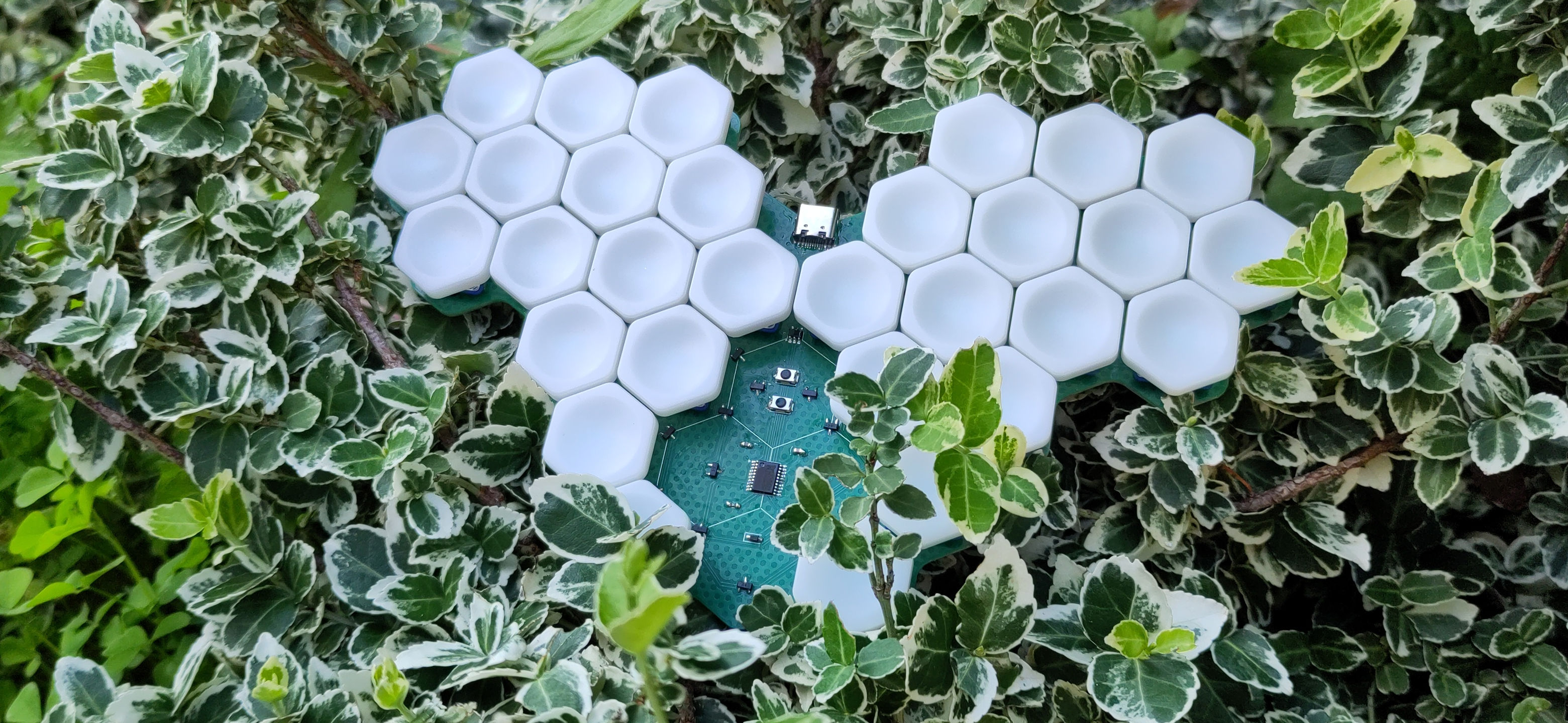
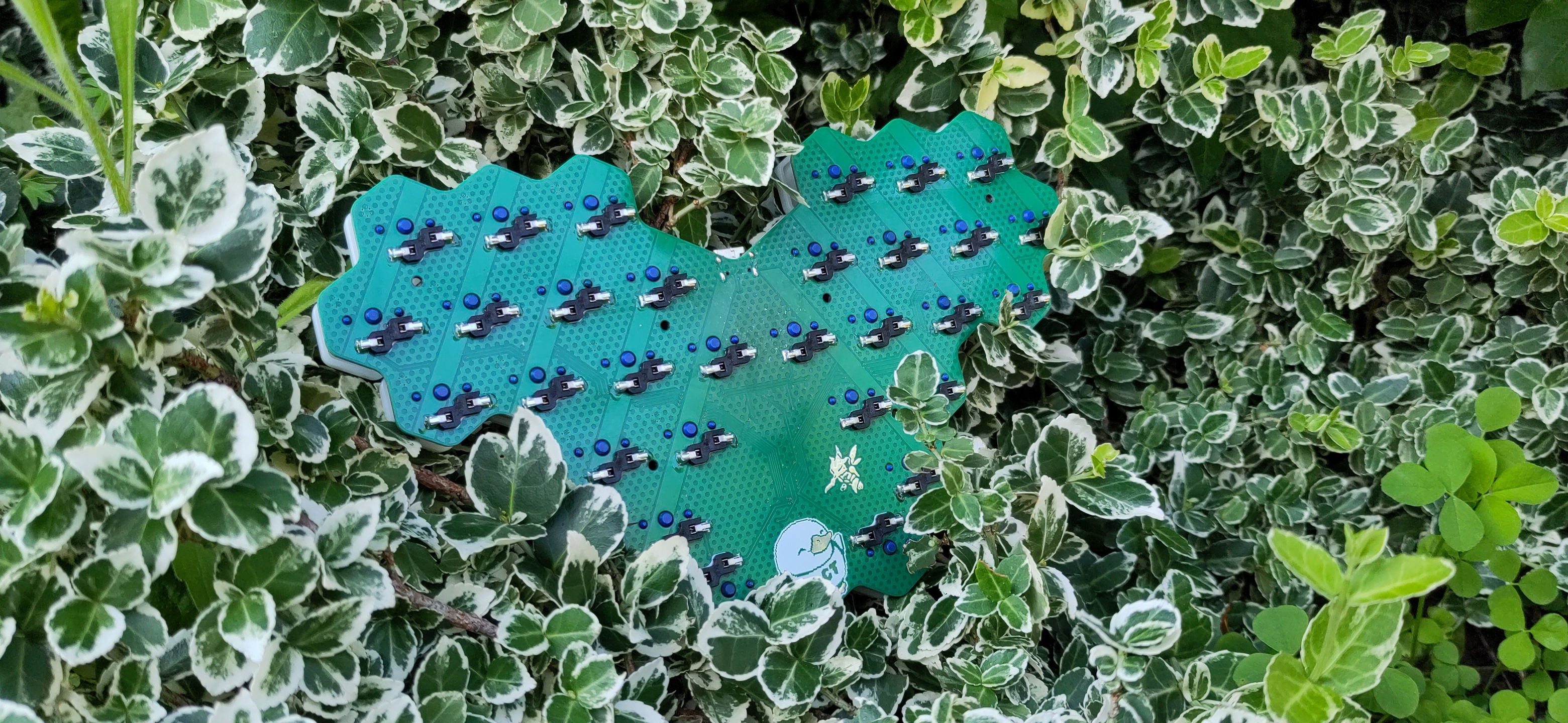
The electronic design is inspired by the MIAO MCU board.
Soldering should be straight forward with the help of the interactive bill of materials
The orientation of U1 and U2 are indicated by small arrows on the PCB.
The orientaion D16 is such that its white line is on the side where the footprint on the silkscreen also has a white line.
For all other components, the orientation does not matter, or their form-factor allows only one orientation (D1-D15).
Make sure to also solder the metal legs on the side, as they will give stability to the jack.
Do not plug in a USB-cabel without soldering the metal legs on the side of the USB-jack! You will most likely rip off the USB-jack when unplugging the USB-cable!
This keyboard is designed for the FAK-firmware.
I've provided some example configuration files in my fork of the fak-config repository with the keyboard name hexapoda.
The push-button closer to the USB-jack is the BOOT button. The one closer to the thumb keys is the RESET button.
| Part | LCSC-Part Nr | amount |
|---|---|---|
| USB-C | C2765186 | 1 |
| CH552T | C111367 | 1 |
| BAV70 Diodes | C727123 | 15 |
| USBLC6-2SC6 | C6807798 | 1 |
| PMEG2010EA | C193668 | 1 |
| Push buttons | C115357 | 2 |
| Fuse | C311055 | 1 |
| 5.1k-Resistor | C23186 | 2 |
| 10k-Resistor | C25804 | 1 |
| 1uF-Capacitor | C2991434 | 2 |
| Hot-Swap-Sockets | 30 | |
| Choc V1 Switches | 30 |
| Qty | Value | Footprint | References |
|---|---|---|---|
| 30 | PG1350 | s-ol:PG1350_hotswap_naked | S1, S2, S10, S11, S12, S13, S14, S15, S16, S17, S18, S19, S20, S21, S22, S23 +14 |
| 15 | BAV70 | silklesspretty:SOT-23 | D1, D2, D3, D4, D5, D6, D7, D8, D9, D10, D11, D12, D13, D14, D15 |
| 6 | MountingHole | MountingHole:MountingHole_2.2mm_M2 | H1, H2, H3, H4, H5, H6 |
| 2 | 100nF | Capacitor_SMD:C_0603_1608Metric_Pad1.08x0.95mm_HandSolder | C1, C2 |
| 2 | 5.1k | Resistor_SMD:R_0603_1608Metric_Pad0.98x0.95mm_HandSolder | R2, R3 |
| 2 | LOGO | LOGO | G***, G*** |
| 1 | 10k | Resistor_SMD:R_0603_1608Metric_Pad0.98x0.95mm_HandSolder | R1 |
| 1 | 500mA | Fuse:Fuse_0603_1608Metric_Pad1.05x0.95mm_HandSolder | F1 |
| 1 | BOOT | Button_Switch_SMD:SW_Push_SPST_NO_Alps_SKRK | SW1 |
| 1 | G*** | kibuzzard-6704E2E6 | kibuzzard-6704E2E6 |
| 1 | PMEG2010EA | Diode_SMD:D_SOD-323_HandSoldering | D16 |
| 1 | RESET | Button_Switch_SMD:SW_Push_SPST_NO_Alps_SKRK | SW2 |
| 1 | USBLC6-2SC6 | Package_TO_SOT_SMD:SOT-23-6 | U2 |
| 1 | USB_C_Receptacle_USB2.0 | Connector_USB:USB_C_Receptacle_HRO_TYPE-C-31-M-12 | J1 |
| 1 | ~ | Package_SO:TSSOP-20_4.4x6.5mm_P0.65mm | U1 |
The 66 most common of 67 parts.
kilipan/miao
A cheap and hand-solderable drop-in replacement for the XIAO using ch552t


tikinson/ToadsTempest
Super small custom 42-keys column-staggered ergonomic mechanical keyboard powered by CH552T microcontroller, created for pocket keyboard design contest #00


chinawrj/FarmMesh-Node
Developing an integrated hardware and software solution for farm-wide Mesh networking: RP2350B/ESP32-C5 nodes, firmware, network protocols, and Wi-Fi/BLE sensor access.

tikinson/kazhan
custom 28-keys ergonomic mechanical keyboard powered by CH552T microcontroller


It measures 193.5 × 116.6 mm and has 2 copper layers, 1.6 mm thick.
67 parts, built around the USBLC6-2SC6, BAV70 and PMEG2010EA. The full list of its parts is on this page, with links to each part's symbol and footprint where PCBKit's library has them.
From the ThePurox/Hexapoda repository on GitHub, at the commit this page was made from: the board is butterfly.kicad_pcb and its schematic butterfly.kicad_sch. PCBKit opens the board in the browser, with nothing to install.
Its repository states no licence, so its author keeps all rights: ask ThePurox before reusing the design.