
6 layers144.8 × 106.7 mm
 suidroot/LevelShifter
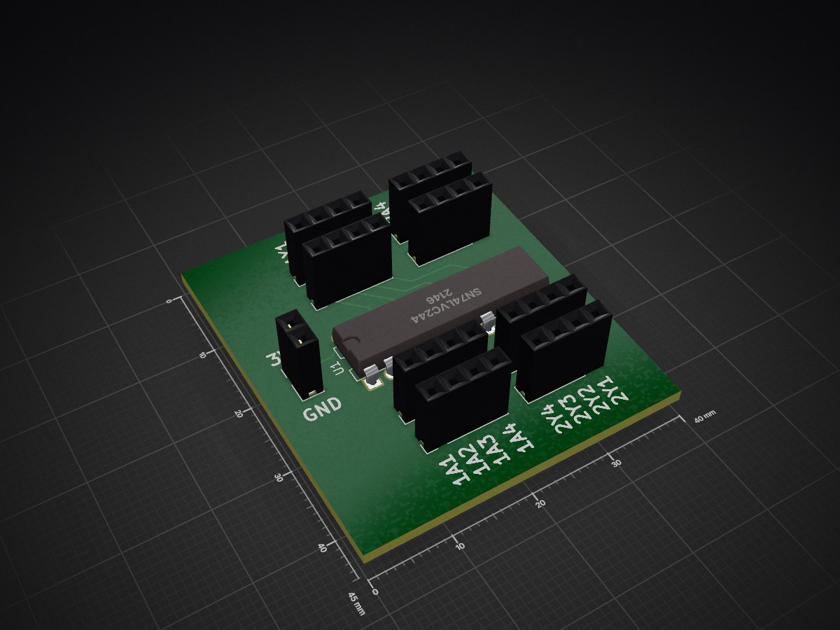
A Board Design for the SN74LVC244 chip to shift from 5v to 3.3v
Level Shifter Board is an open-source printed circuit board by suidroot, from the suidroot/LevelShifter repository on GitHub. It is a 2-layer board of 40 × 45 mm with 10 parts on 18 nets, routed with 58 tracks and 0 vias.
It is built around the SN74LVC244AN. Its parts include 9 connectors and 1 IC. It belongs with the interfaces and adapters boards of this library.
A Board Design for the SN74LVC244 chip to shift from 5v to 3.3v
This design was built out in Kicad
| Qty | Value | Footprint | References |
|---|---|---|---|
| 8 | CONN_01X04 | Socket_Strips:Socket_Strip_Straight_1x04_Pitch2.54mm | P1, P2, P4, P5, P6, P7, P8, P9 |
| 1 | CONN_01X02 | Socket_Strips:Socket_Strip_Straight_1x02_Pitch2.54mm | P3 |
| 1 | SN74LVC244 | Housings_DIP:DIP-20_W7.62mm | U1 |
It measures 40 × 45 mm and has 2 copper layers, 1.6 mm thick.
10 parts, built around the SN74LVC244AN. The full list of its parts is on this page, with links to each part's symbol and footprint where PCBKit's library has them.
From the suidroot/LevelShifter repository on GitHub, at the commit this page was made from: the board is Level Shifter Board.kicad_pcb. PCBKit opens the board in the browser, with nothing to install.
Its repository states no licence, so its author keeps all rights: ask suidroot before reusing the design.

GLGPrograms/tinyDiskII
Homemade floppy disk emulator for Apple II series computers

auselia/adc_test_board
ADS7057 test board: perfboard SMA -> filters -> ADC + wake comparator -> ZedBoard PMOD (KiCad 10, JLCPCB-ready)


gloveboxes/pcb-z80
pcb-z80 is a container-only, repeatable build of the four-layer Z80 ROMless SBC PCB engineering design. It regenerates the KiCad schematic, places the four-layer board, routes a fresh Specctra session, imports and fills…

MicroCoreLabs/Projects
Ted Fried's MicroCore Labs Projects - FPGA CPU cores and emulators for the 8088, 8086, 8051, 6502, 68000, Z80, Risc-V, and also Typewriter and EPROM Emulator projects.

gloveboxes/Z80ROMlessSBC
This is a separate KiCad project for a 98.3 × 60 mm, four-layer board. JLCPCB assembles every top-side SMT part, including the Raspberry Pi Pico 2 W module, and only four parts are hand-soldered:

gusmanb/logicanalyzer
24 channel, 100Msps logic analyzer hardware and software