4 layers194.3 × 92.8 mm
 sufst/pcb19
Monorepo for all schematics and PCB designs
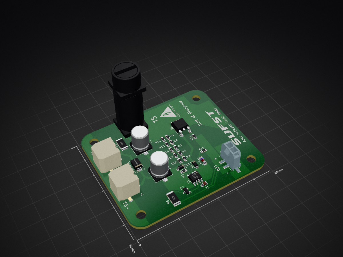
Ail is an open-source printed circuit board by sufst, from the sufst/pcb repository on GitHub, published under the GPL-3.0 licence. It is a 2-layer board of 69 × 58 mm with 35 parts on 28 nets, routed with 83 tracks and 0 vias.
It is built around the 0461.500ER, BZV55B6V2 and IPD80R4K5P7, with the MMSZ4699T1G-TP, MMSZ5239B and P6SMB440CA among its other parts. Its parts include 15 resistors, 4 diodes, 3 capacitors, 3 connectors and 2 transistors.


Central repository of all schematics and PCB design files.
| Folder | Project | Project Code |
|---|---|---|
| ail | Accumulator Indicator Light Logic | ail |
| ail-led | Accumulator Indicator Light Led | ail-led |
| batak | Batak Game (non-car) | batak |
| break-light | Rear Break Light | break-light |
| bspd | Brake System Plausibility Device | bspd |
| can-node | Voltage Reader and Broadcaster | can-node |
| curr-amp | Current Sensor Amplifier | curr-amp |
| dash | Dashboard | dash |
| discharge | Discharge Relay Breakout | discharge |
| hv-sense | High Voltage Sense | hvs |
| latching | Latch Circuit | latching |
| loom* | Loom Design | loom |
| lvbms | Low Voltage Battery Management System | lvbms |
| precharge | Precharge Controller | precharge |
| segment | Segment | segment |
| telemetry | On-Car Telemetry | telemetry |
| test-rig | PCB Test / Demo Rig | test |
| top-level* | Full Car Schematic | |
| trc | TSAC Relay Controller | trc |
| tsal | Tractive System Active Light | tsal |
| vcu | Vehicle Control Unit | vcu |
We design our PCBs in KiCad (version 8+).
*Moved to https://github.com/sufst/loom
Files that should be in this repo, under version control:
.kicad_pro)..kicad_sch)..kicad_pcb)..kicad_mod)..kicad_sym).fp-lib-table).sym-lib-table)..step files)..asc files from LTSpice).Files that should never be in here:
.kicad_prl).<project name>-backups, .bak .bck -bak files).fp-info-cache).The .gitignore should prevent the addition of files we don't want to keep in here, but before you commit make sure to do a quick check of what is actually being added.
The common folder is used for resources which can be shared across multiple projects. This includes:
images subdirectory).step subdirectory).sufst-lib.kicad_sym).sufst-lib.pretty).sheet-layout.kicad_wks).Note: Since projects were previously in their own individual repos, many designs still have their own libraries, step files, etc. These will gradually be migrated to the SUFST library.
When you configure the library paths for a project (sym-lib-table and fp-lib-table data), make sure to always use a path relative to the project with the ${KIPRJMOD} substitution.
${KIPRJMOD}/../common/sufst-lib.kicad_sym/Users/<your name>/Documents/sufst/pcb/common/sufst-lib.kicad_symIf an absolute path is used, when someone else opens the project that path will not exist and the library paths will not be valid. -lib-table files should never contain an absolute path.
It is not possible to resolve merge conflicts within individual design files, which is an unfortunate limitation of using git with KiCad. While KiCad files are in a text format, they aren't really designed to be edited manually. It is therefore essential that only one person is editing a particular file in a project at a time (including the shared library). Once someone starts working on a file, until it is merged into the main branch nobody else can edit that file. A good way to get round this is to use the "hierarchical sheets" feature to divide schematics into multiple files (if it can be done in a logical way).
When a PCB is fabricated, a new 'release' for the given project should be
created and stored within this repo in the releases/<PROJECT NAME> folder.
This folder should contain the latest version (and ONLY the latest version) of
the following files:
fabrication.zip.Schematic.pdf).Layout.pdf).ibom.html).Additionally, a file called info (no extension) should be created (if it
doesn't already exist) containing release information in the following format:
version: <VERSION NUMBER>
date: <RELEASE DATE>
fabrication: <COMPANY>
Version numbers should be in the format v1.0.1 and dates should be in the
format YYYY-MM-DD. For example:
version: v1.0.1
date: 2023-01-23
fabrication: JLCPCB
The release folder for a project should then have the following structure and file names:
<PROJECT NAME>
├── Layout.pdf
├── Schematic.pdf
├── fabrication.zip
├── ibom.html
└── info
When creating a new release, make sure to overwrite/replace all the existing files.
The release commit should then be tagged with the following command:
git tag <PROJECT CODE>-<VERSION_NUMBER>Tagging should be done after merging to main! Example command:
git tag segment-v1.0.1To push tags to GitHub:
git push --tags| Qty | Value | Footprint | References |
|---|---|---|---|
| 9 | 200k | Resistor_SMD:R_0805_2012Metric_Pad1.20x1.40mm_HandSolder | R1, R2, R3, R4, R5, R12, R13, R14, R15 |
| 4 | MountingHole | MountingHole:MountingHole_4.3mm_M4 | H1, H2, H3, H4 |
| 2 | 2.7u | Capacitor_SMD:C_Elec_8x10.2 | C2, C3 |
| 1 | 0461.500ER | SUFST:Littelfuse-04611-25ER | F1 |
| 1 | 100 | Resistor_SMD:R_0805_2012Metric_Pad1.20x1.40mm_HandSolder | R11 |
| 1 | 100k | Resistor_SMD:R_0805_2012Metric_Pad1.20x1.40mm_HandSolder | R16 |
| 1 | 100n | Capacitor_SMD:C_0805_2012Metric_Pad1.18x1.45mm_HandSolder | C1 |
| 1 | 110k | Resistor_SMD:R_0805_2012Metric_Pad1.20x1.40mm_HandSolder | R9 |
| 1 | 1k | Resistor_SMD:R_2512_6332Metric | R19 |
| 1 | 4.7k | Resistor_SMD:R_0805_2012Metric_Pad1.20x1.40mm_HandSolder | R10 |
| 1 | 470 | Resistor_SMD:R_2512_6332Metric_Pad1.40x3.35mm_HandSolder | R8 |
| 1 | BZV55B6V2 | Diode_SMD:D_MiniMELF | D2 |
| 1 | HV_TRIANGLE_SYMBOL | SUFST:HV_TRIANGLE_SYMBOL | G*** |
| 1 | IPD80R4K5P7 | Package_TO_SOT_SMD:TO-252-2 | Q1 |
| 1 | LED | Connector_Molex:Molex_Micro-Fit_3.0_43650-0224_1x02-1MP_P3.00mm_Vertical | J3 |
| 1 | LOGO | SUFST:sufst-text | G*** |
| 1 | MMSZ4699T1G | Diode_SMD:D_SOD-123 | D1 |
| 1 | MMSZ5239B | Diode_SMD:D_SOD-123 | D3 |
| 1 | OP777 | Package_SO:SOIC-8_3.9x4.9mm_P1.27mm | U1 |
| 1 | P6SMB440CA | PCM_Diode_SMD_AKL:D_SMB_TVS | D4 |
| 1 | TS HV+ | SUFST:Molex_Micro-Fit_3.0_43650-0214_1x02_P3.00mm_Horizontal | J1 |
| 1 | TS HV- | SUFST:Molex_Micro-Fit_3.0_43650-0214_1x02_P3.00mm_Horizontal | J2 |
| 1 | XP262N7002TR-G | Package_TO_SOT_SMD:SOT-23 | Q2 |
It measures 69 × 58 mm and has 2 copper layers, 1.6 mm thick.
35 parts, built around the 0461.500ER, BZV55B6V2, IPD80R4K5P7 and MMSZ4699T1G-TP. The full list of its parts is on this page, with links to each part's symbol and footprint where PCBKit's library has them.
From the sufst/pcb repository on GitHub, at the commit this page was made from: the board is ail/ail.kicad_pcb. PCBKit opens the board in the browser, with nothing to install.
Its repository publishes it under the GPL-3.0 licence: you may reuse it on that licence's terms (keep the author's notice, and for a copyleft licence share your changes alike).


Rr42/USB-C-DB
Demo board for testing and evaluating the USB-C interface for Micro-controllers with onboard battery charging.

czalinski/ThlHwTestDevices
KiCad designs, firmware and documentation for circuits that support testing of electrical hardware, such as HASS and HALT testing.

hackclub/OnBoard
💡 Join 1,000 teenagers and make your first PCB with a $100 grant!


ozel/DIY_particle_detector
A mobile low-cost spectrometer for measuring radioactivity and the energy of ionising radiation like alpha particles and electrons

Seeed-Studio/OSHW-reCamera-Series
reCamera is a series of open-source AI cameras.

