4 layers89 × 89.5 mm
SDR v3-TayloeDetector FINAL
JDPennockGB/ENGR357-SDR-PennockRoque
A custom-built, high-performance Software Defined Radio (SDR) receiver powered by the Raspberry Pi Pico (RP2040).
120 parts1

 SomethingFourier/SDR-Receiver3
Super Heterodyne Direct Conversion Hybrid I/Q SDR Receiver
Diode tayloe sdr is an open-source printed circuit board by SomethingFourier, from the SomethingFourier/SDR-Receiver repository on GitHub. It is a 4-layer board of 99.7 × 99.7 mm with 279 parts on 185 nets, routed with 1,947 tracks and 665 vias.
It is built around the ADE-1+, CJC5340 and AP7361C-33E, with the LM66100DCK, AG9905LP and 1N4004W among its other parts. Its parts include 112 capacitors, 52 resistors, 16 ICs, 12 inductors and 9 diodes. It belongs with the radio and wireless boards of this library.


Hybrid Super Heterodyne Direct Conversion I/Q SDR Receiver
An open-source, hybrid-architecture Software Defined Radio (SDR) receiver built around the RP2350 microcontroller. This project blends superheterodyne and direct-conversion (Tayloe detector) techniques. It's been designed to listen to the 2-meter band, but covers a tunable range of 5 MHz to 160 MHz. It features both USB-C (USB 1.1) and Ethernet data communication, as well as Power over Ethernet (PoE) capabilities. Ethernet streaming is currently functional but still under active development and not yet ready for final deployment.
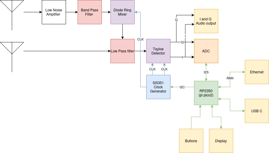
The receiver is divided into distinct HF and VHF signal paths. Each path utilizes a dedicated antenna equipped with an isolation transformer to prevent ground loops.
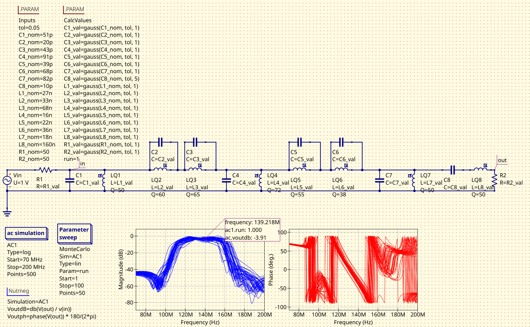
A multiplexer selects between the HF signal and the down-converted VHF signal, feeding the active path into a shared low-pass filter.
After the low-pass filter, the signal makes its way to the Tayloe detector. The Tayloe detector mixes the signal down to be centered at 0 Hz with both an in-phase and a quadrature output. These I and Q outputs are then fed into the analog-to-digital converter. As this is a first revision board, as a backup and insurance measure, we've also connected the I and Q outputs to a 3.5 mm jack for use with an external sound card.
The whole SDR is built around the RP2350 microcontroller. The RP2350 will talk to SDR software either over a USB-C or Ethernet connection. It will receive commands to change the tuning frequency, and relay that information to the clock generator for this SDR, the Si5351-compatible MS5351M. It will also interface with a small I2C OLED display and a couple of buttons for a local user interface. It will receive the SDR I and Q data from the ADC via I2S, and send that data over either the USB-C or Ethernet connection to the computer running the SDR software.
| GPIO Pin | Function | Subsystem |
|---|---|---|
| 0 - 1 | I2C SDA / I2C SCL | I2C |
| 2 - 3 | Select button / Enter button | UI Buttons |
| 4 | Red LED | LED |
| 5 | Green LED | LED |
| 6 - 7 | ADC M0 / ADC M1 | ADC Mode |
| 8 | VHF BP Filter Mux select | Mux Selects |
| 9 | Mux U18 Select | Mux Selects |
| 10 - 12 | Ethernet TX Enable, TXD0, TXD1 | Eth TX (Programmable IO) |
| 13 - 15 | Ethernet Carrier Sense/Data Valid, RXD0, RXD1 | Eth RX (Programmable IO) |
| 16 - 18 | LAN8720A Management Data I/O, CLK, Reset | Eth Manage (Programmable IO) |
| 19 - 21 | I2S CLK, Word Select, Data | I2S (Programmable IO) |
| 22 | Extra GPIO | General |
| 23 | Ethernet 50 MHz Clk output | Programmable IO |
| 24 - 25 | Extra GPIO | General |
| 26 | White LED | LED |
| 27 - 28 | Extra GPIO | General |
| 29 | Yellow LED | LED |
| 56 - 60 | QSPI (SCLK, SDO, SD1-3, SS) | Flash Memory |
(Note: Pin mapping is subject to change as the board layout is finalized. Refer to pico.kicad_sch for the raw schematic).
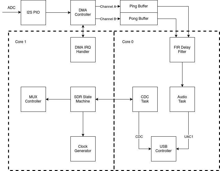
The firmware runs on both cores of the RP2350 simultaneously, dividing responsibilities between real-time data acquisition/DSP (Core 0) and hardware control (Core 1).
I/Q samples from the ADC are clocked in over I2S using a PIO state machine. A DMA controller with two channels shuttles those samples into a ping-pong buffer pair — while one buffer is being filled (e.g., Ping), the other (Pong) is available for processing. When a transfer completes, a DMA IRQ handler on Core 1 signals Core 0 to begin processing the newly filled buffer, then arms the next DMA transfer into the opposite buffer.
On Core 0, the freshly filled buffer is passed through a FIR delay filter before being handed to the Audio Task. The FIR filter compensates for the ADC clone's fixed channel skew (about 1.9 microseconds between left and right channels), aligning I/Q timing before streaming. The Audio Task packages the filtered I/Q samples and feeds them to the USB Controller as a UAC1 (USB Audio Class 1) stream, making the SDR appear as a standard USB audio device to any SDR application running on the host.
A separate CDC Task on Core 0 monitors the USB CDC (virtual serial port) interface for incoming commands from the host. Commands are forwarded to the SDR State Machine on Core 1, which acts as the central coordinator for hardware control. In response, the state machine drives:
Ethernet software is currently available in development form and can work, but it remains unreliable and is not considered deployment-ready.
The bidirectional arrow between the CDC Task and the SDR State Machine also allows the state machine to send status back to the host over the CDC interface.
| Core | Responsibilities |
|---|---|
| Core 0 | FIR filtering, Audio Task (UAC1 streaming), CDC Task (command parsing) |
| Core 1 | DMA IRQ handling, SDR State Machine, Clock Generator (I2C), MUX control |
The firmware uses CMake with the Raspberry Pi Pico SDK.
arm-none-eabi-gcc)Set the Pico SDK path before configuring:
export PICO_SDK_PATH=/path/to/pico-sdkcd firmware
mkdir -p build
cd build
cmake ..
cmake --build . -jThe firmware image is generated as sdr.uf2 in the build output directory.
sdr.uf2 onto that device.The first order of boards arrived and we worked through our board bring-up plan to safely get our board working, finding any errors we may have made. The following issues were discovered.
| Qty | Value | Footprint | References |
|---|---|---|---|
| 33 | 100nF | PCM_JLCPCB:C_0402 | C13, C19, C21, C33, C35, C37, C39, C41, C42, C101, C103, C105, C107, C110, C114, C120 +17 |
| 16 | 100pF | PCM_JLCPCB:C_0603 | C32, C73, C76, C77, C85, C86, C90, C93, C94, C100, C102, C104, C108, C111, C112, C115 |
| 13 | 10kΩ | PCM_JLCPCB:R_0402 | R6, R10, R16, R17, R20, R22, R25, R27, R28, R32, R33, R35, R46 |
| 12 | 10uF | PCM_JLCPCB:C_0603 | C7, C9, C10, C34, C60, C67, C75, C78, C91, C96, C109, C113 |
| 12 | SolderJumper_2_Open | Jumper:SolderJumper-2_P1.3mm_Open_Pad1.0x1.5mm | JP5, JP6, JP11, JP13, JP15, JP16, JP19, JP20, JP23, JP24, JP25, JP31 |
| 10 | 1uF | PCM_JLCPCB:C_0402 | C36, C38, C40, C43, C45, C50, C52, C82, C84, C119 |
| 10 | 4.7uF | PCM_JLCPCB:C_0402 | C11, C15, C16, C18, C20, C22, C23, C24, C25, C88 |
| 7 | ~ | Jumper:SolderJumper-2_P1.3mm_Bridged_RoundedPad1.0x1.5mm | JP10, JP18, JP26, JP27, JP28, JP29, JP30 |
| 6 | SolderJumper_2_Bridged | Jumper:SolderJumper-2_P1.3mm_Bridged_RoundedPad1.0x1.5mm | JP3, JP4, JP12, JP14, JP21, JP22 |
| 4 | 100kΩ | PCM_JLCPCB:R_0402 | R44, R45, R49, R50 |
| 4 | 100nF | PCM_JLCPCB:C_0805 | C12, C46, C47, C48 |
| 4 | 100Ω | PCM_JLCPCB:R_0402 | R30, R31, R36, R39 |
| 4 | 10nF | PCM_JLCPCB:C_0603 | C1, C2, C3, C4 |
| 4 | 1N4004W | PCM_JLCPCB:D_SOD-123FL | D9, D10, D11, D12 |
| 4 | 33Ω | PCM_JLCPCB:R_0805 | R34, R37, R38, R42 |
| 4 | AP7361C-33E | Package_TO_SOT_SMD:SOT-223-3_TabPin2 | U24, U25, U26, U27 |
| 4 | MountingHole | MountingHole:MountingHole_3.2mm_M3 | H1, H2, H3, H4 |
| 4 | Tactile Button, 160gf | PCM_JLCPCB:SW_TS-1088-AR02016 | S1, S2, S3, S4 |
| 3 | 1kΩ | PCM_JLCPCB:R_0402 | R2, R5, R7 |
| 3 | 330Ω | PCM_JLCPCB:R_0402 | R11, R12, R19 |
| 3 | 43pF 1% | PCM_JLCPCB:C_0402 | C80, C81, C89 |
| 3 | 91pF | PCM_JLCPCB:C_0402 | C61, C65, C66 |
| 3 | LM66100DCK | Package_TO_SOT_SMD:SOT-363_SC-70-6 | U13, U14, U15 |
| 3 | OPA1612AxD | Package_SO:SOIC-8_3.9x4.9mm_P1.27mm | U2, U3, U8 |
| 3 | ~ | EasyEDA_Lib:SOT-23-6_L2.9-W1.6-P0.95-LS2.8-BR | U17, U18, U19 |
| 3 | ~ | PCM_JLCPCB:FB_0805 | FB1, FB2, FB4 |
| 2 | 1.5kΩ | PCM_JLCPCB:R_0805 | R29, R40 |
| 2 | 100uF 25V | Capacitor_SMD:CP_Elec_6.3x7.7 | C72, C116 |
| 2 | 10kΩ | PCM_JLCPCB:R_0805 | R21, R41 |
| 2 | 10pF | PCM_JLCPCB:C_0402 | C6, C49 |
| 2 | 2.2nF | PCM_JLCPCB:C_1206 | C106, C121 |
| 2 | 27Ω | PCM_JLCPCB:R_0603 | R8, R9 |
| 2 | 33pF | PCM_JLCPCB:C_0402 | C14, C17 |
| 2 | 3GHz | EasyEDA_Lib:BNC-TH_DOSIN-801-0051 | RF1, RF2 |
| 2 | 4.7kΩ | PCM_JLCPCB:R_0402 | R23, R24 |
| 2 | 470pF | PCM_JLCPCB:C_0805 | C69, C79 |
| 2 | 47Ω | PCM_JLCPCB:R_0402 | R14, R15 |
| 2 | 5.1kΩ | PCM_JLCPCB:R_0402 | R1, R4 |
| 2 | 634Ω | PCM_JLCPCB:R_0402 | R48, R51 |
| 2 | 91Ω | PCM_JLCPCB:R_0402 | R47, R52 |
| 2 | Jumper_2_Small_Open | Connector_PinHeader_2.54mm:PinHeader_1x02_P2.54mm_Vertical | JP2, JP17 |
| 2 | LOGO | LOGO | G***, G*** |
| 2 | MB10S | sdr_project:SOIC245P670X290-4N | D3, D4 |
| 2 | Red | PCM_JLCPCB:D_0603 | D1, D5 |
| 1 | 1.5kΩ | PCM_JLCPCB:R_0402 | R26 |
| 1 | 10uF | PCM_JLCPCB:C_0402 | C68 |
| 1 | 12kΩ | PCM_JLCPCB:R_0402 | R18 |
| 1 | 160nH | PCM_JLCPCB:L_0805 | L10 |
| 1 | 16nH | EasyEDA_Lib:IND-SMD_L2.4-W1.7 | L6 |
| 1 | 18nH | EasyEDA_Lib:IND-SMD_L2.2-W1.6 | L9 |
| 1 | 2.2uH,50mA | PCM_JLCPCB:L_0805 | L12 |
| 1 | 20pF | PCM_JLCPCB:C_0402 | C59 |
| 1 | 22nH | sdr_project:L_APV_AHW2520 | L7 |
| 1 | 27nH | Inductor_SMD:L_1210_3225Metric | L3 |
| 1 | 300nH | PCM_JLCPCB:L_0805 | L11 |
| 1 | 33nH | EasyEDA_Lib:IND-SMD_L2.2-W1.6 | L4 |
| 1 | 33Ω | PCM_JLCPCB:R_0402 | R13 |
| 1 | 36nH | PCM_JLCPCB:L_0603 | L8 |
| 1 | 39pF | PCM_JLCPCB:C_0402 | C62 |
| 1 | 4.7uH,25mA | PCM_JLCPCB:L_1206 | L2 |
| 1 | 47 1% | PCM_JLCPCB:R_0603 | R43 |
| 1 | 470pF | PCM_JLCPCB:C_0402 | C51 |
| 1 | 47kΩ | PCM_JLCPCB:R_0402 | R3 |
| 1 | 5.65V Jumper | Jumper:SolderJumper-2_P1.3mm_Bridged_RoundedPad1.0x1.5mm | JP1 |
| 1 | 51pF | PCM_JLCPCB:C_0402 | C58 |
| 1 | 68nH | Inductor_SMD:L_1008_2520Metric | L5 |
| 1 | 68pF | PCM_JLCPCB:C_0402 | C63 |
| 1 | 82pF | PCM_JLCPCB:C_0402 | C64 |
| 1 | ADE-1+ | sdr_project:ADE12 | U5 |
| 1 | AOTA-B201610S3R3-101-T | EasyEDA_Lib:IND-SMD_L2.0-W1.6_AOTA-B201610S3R3-101-T | L1 |
| 1 | Ag9905LP | Converter_DCDC:Converter_DCDC_Silvertel_Ag99xxLP_THT | U11 |
| 1 | CJC5340 | Package_SO:TSSOP-16_4.4x5mm_P0.65mm | U4 |
| 1 | DC_Jumper | Jumper:SolderJumper-2_P1.3mm_Bridged_RoundedPad1.0x1.5mm | JP8 |
| 1 | Debug Pins | Connector_PinHeader_2.54mm:PinHeader_1x03_P2.54mm_Vertical | J4 |
| 1 | Display Connector | Connector_PinHeader_2.54mm:PinHeader_1x04_P2.54mm_Vertical | J5 |
| 1 | External Filter | Connector_PinHeader_2.54mm:PinHeader_1x04_P2.54mm_Vertical | J3 |
| 1 | Extra GPIO | Connector_PinHeader_2.54mm:PinHeader_1x05_P2.54mm_Vertical | J8 |
| 1 | GND | TestPoint:TestPoint_Pad_1.5x1.5mm | TP8 |
| 1 | Green | PCM_JLCPCB:D_0805 | D13 |
| 1 | H1102NLT | sdr_project:XFMR_H1102NLT | T1 |
The 251 most common of 279 parts.
It measures 99.7 × 99.7 mm and has 4 copper layers, 1.6 mm thick.
279 parts, built around the ADE-1+, CJC5340, AP7361C-33E and LM66100DCK. The full list of its parts is on this page, with links to each part's symbol and footprint where PCBKit's library has them.
From the SomethingFourier/SDR-Receiver repository on GitHub, at the commit this page was made from: the board is kicad/diode_tayloe_sdr.kicad_pcb and its schematic kicad/.kicad_sch. PCBKit opens the board in the browser, with nothing to install.
Its repository states no licence, so its author keeps all rights: ask SomethingFourier before reusing the design.
JDPennockGB/ENGR357-SDR-PennockRoque
A custom-built, high-performance Software Defined Radio (SDR) receiver powered by the Raspberry Pi Pico (RP2040).

colinoflynn/phase-modulation-sca
Resources to demonstrate phase modulation leakage including over JTAG

mpkendall/phase-interferometer
A 2(or more)-element phase interferometric direction finder for 433 MHz using a passive phased array

ngrabbs/ember
Open pvpanel.kicadpro with KiCad 10. The project contains the recovered schematic, routed PCB, project-local footprint libraries, and solar-module STEP model.


mahdi-kh1265/mts-electronics
Analog RF, photodetector, and demodulation electronics for POSM's modulation-transfer spectroscopy (MTS) laser-locking system.

