
2 layers
CourseWorkScheme
NasterVill/BSUIR_Labs
Here are gathered all the labs from my CMSnN studying course.
40 parts27Apache-2.0

 shyver/Precision-Light-Sensor-AFE
Designed as a modular Analog Front-End (AFE), this board converts ambient light intensity into a clean, stable analog voltage (0–3.3V) suitable for direct sampling by microcontrollers (e.g., ESP32, STM32, Arduino) using…
Photodiode TIA is an open-source printed circuit board by shyver, from the shyver/Precision-Light-Sensor-AFE repository on GitHub, published under the MIT licence. It is a 2-layer board of 25 × 10 mm with 8 parts on 5 nets, routed with 26 tracks and 1 via.
It is built around the MCP6001R-I/OT and BPW34. Its parts include 3 capacitors, 2 resistors, 1 IC, 1 diode and 1 connector.



This repository contains the hardware design files and LTspice simulations for a high-precision, low-noise Photodiode Signal Conditioning Board.
Designed as a modular Analog Front-End (AFE), this board converts ambient light intensity into a clean, stable analog voltage (0–3.3V) suitable for direct sampling by microcontrollers (e.g., ESP32, STM32, Arduino) using a Transimpedance Amplifier (TIA) architecture.
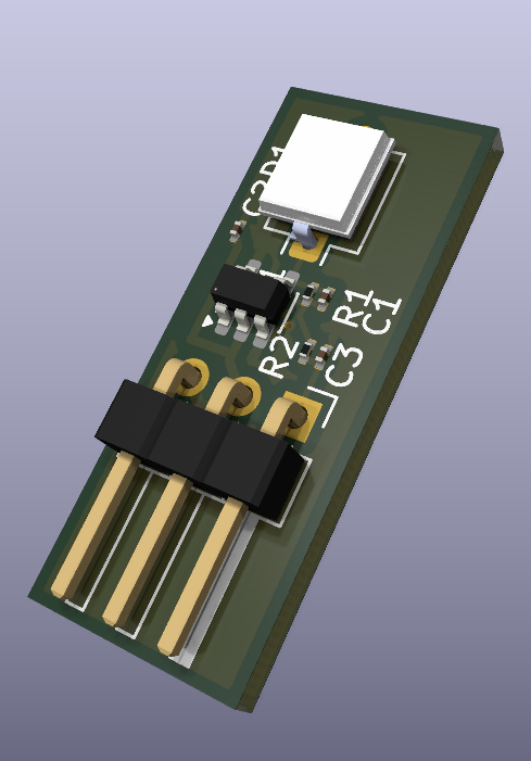
| Component | Part / Value | Description |
|---|---|---|
| Photodiode | BPW34S | Broadband silicon photodiode. High photocurrent (~50µA at 1000 Lux), low dark current (2nA). |
| Op-Amp | MCP6001 | Single-supply, Rail-to-Rail Output (RRO), CMOS input (1pA Bias Current). |
| Gain Resistor ($R_f$) | 68 kΩ | Sets the voltage output range (Max 3.3V at ~50µA input). |
| Compensation Cap ($C_f$) | 20 pF | Prevents ringing/oscillation caused by the photodiode's 72pF junction capacitance. |
| Supply Voltage | 3.3V | Single-supply operation. Decoupled via 0.1µF capacitor. |
The BPW34S photodiode is operated in photovoltaic/zero-bias mode. This configuration minimizes dark current leakage, resulting in the highest possible precision and lowest noise floor for ambient light detection.
The core of the board is the TIA. The gain is set by the feedback resistor ($R_f$). Using Ohm's Law ($V = I \times R$), a peak ambient room light producing $~50 \mu A$ of current is multiplied by $68 k\Omega$ to produce a $~3.4V$ output, perfectly utilizing the 3.3V ADC range of modern microcontrollers.
Photodiodes with large active areas (like the BPW34S) have high junction capacitance ($C_j \approx 72pF$). Without compensation, this capacitance creates a phase shift in the op-amp's feedback loop, causing severe ringing and instability. A 20pF feedback capacitor ($C_f$) was mathematically calculated and verified via SPICE simulation to critically damp the circuit and provide a smooth transient response.
/kicad - KiCad 9.0 project files (Schematic, PCB Layout, Footprints)./Simulation - LTspice .asc files demonstrating Transient and AC (Frequency Response) analysis./Docs - Datasheets for the BPW34S and MCP6001./Manufacturing - Gerber files, Drill files, and BOM ready for PCB manufacturing (e.g., JLCPCB)./Media - Project media and screenshots.git clone https://github.com/shyver/Precision-Light-Sensor-AFE.git.pro or .kicad_pro file in KiCad..asc files located in the /Simulation folder using LTspice.This project is open-source and available under the MIT License.
| Qty | Value | Footprint | References |
|---|---|---|---|
| 1 | 0.1µ | Capacitor_SMD:C_0201_0603Metric | C2 |
| 1 | 100 | Resistor_SMD:R_0201_0603Metric | R2 |
| 1 | 10n | Capacitor_SMD:C_0201_0603Metric | C3 |
| 1 | 20p | Capacitor_SMD:C_0201_0603Metric | C1 |
| 1 | 68k | Resistor_SMD:R_0201_0603Metric | R1 |
| 1 | BPW34 | OptoDevice:Osram_DIL2_4.3x4.65mm_P5.08mm | D1 |
| 1 | Conn_01x03_Pin | Connector_PinHeader_2.54mm:PinHeader_1x03_P2.54mm_Horizontal | J3 |
| 1 | MCP6001R | Package_TO_SOT_SMD:SOT-23-5 | U1 |
It measures 25 × 10 mm and has 2 copper layers, 1.6 mm thick.
8 parts, built around the MCP6001R-I/OT and BPW34. The full list of its parts is on this page, with links to each part's symbol and footprint where PCBKit's library has them.
From the shyver/Precision-Light-Sensor-AFE repository on GitHub, at the commit this page was made from: the board is kicad/photodiode_TIA/photodiode_TIA.kicad_pcb and its schematic kicad/photodiode_TIA/photodiode_TIA.kicad_sch. PCBKit opens the board in the browser, with nothing to install.
Its repository publishes it under the MIT licence: you may reuse it on that licence's terms (keep the author's notice, and for a copyleft licence share your changes alike).
NasterVill/BSUIR_Labs
Here are gathered all the labs from my CMSnN studying course.

iotmakervn/iot-wifi-uno-hw
Open hardware ESP8266 Uno board - Internet Of Things WiFi Uno


AlexW-proj/ion-pump-controller
open source controller that takes 24V in and spits out 0 - 7000V, set by a knob with an adjustable ramp time

jacoblinnabary/JCOBB-Controller-Board
Analog PWM generator for RC/drone control. Produces 1–2 ms pulses at a 20 ms frame using an RC ramp and comparator.

melikeatilgan/asenkron-motor-bakim
15 kW asenkron motor için arıza ağacı analizi, aylık bakım formu ve KiCad'de tasarlanmış üç izleme kartı

