

4 layers99 × 53.3 mm
PSLab
fossasia/pslab-hardware
PSLab Hardware Design and Schematics https://pslab.io
199 parts1.7kApache-2.0

MeEC is an open-source printed circuit board by sekigon-gonnoc, from the sekigon-gonnoc/meEC repository on GitHub, published under the MIT licence. It is a 2-layer board of 91 × 55 mm with 18 parts on 30 nets, routed with 111 tracks and 129 vias.
It is built around the WS2812B. Its parts include 5 switches, 4 diodes and 1 IC.
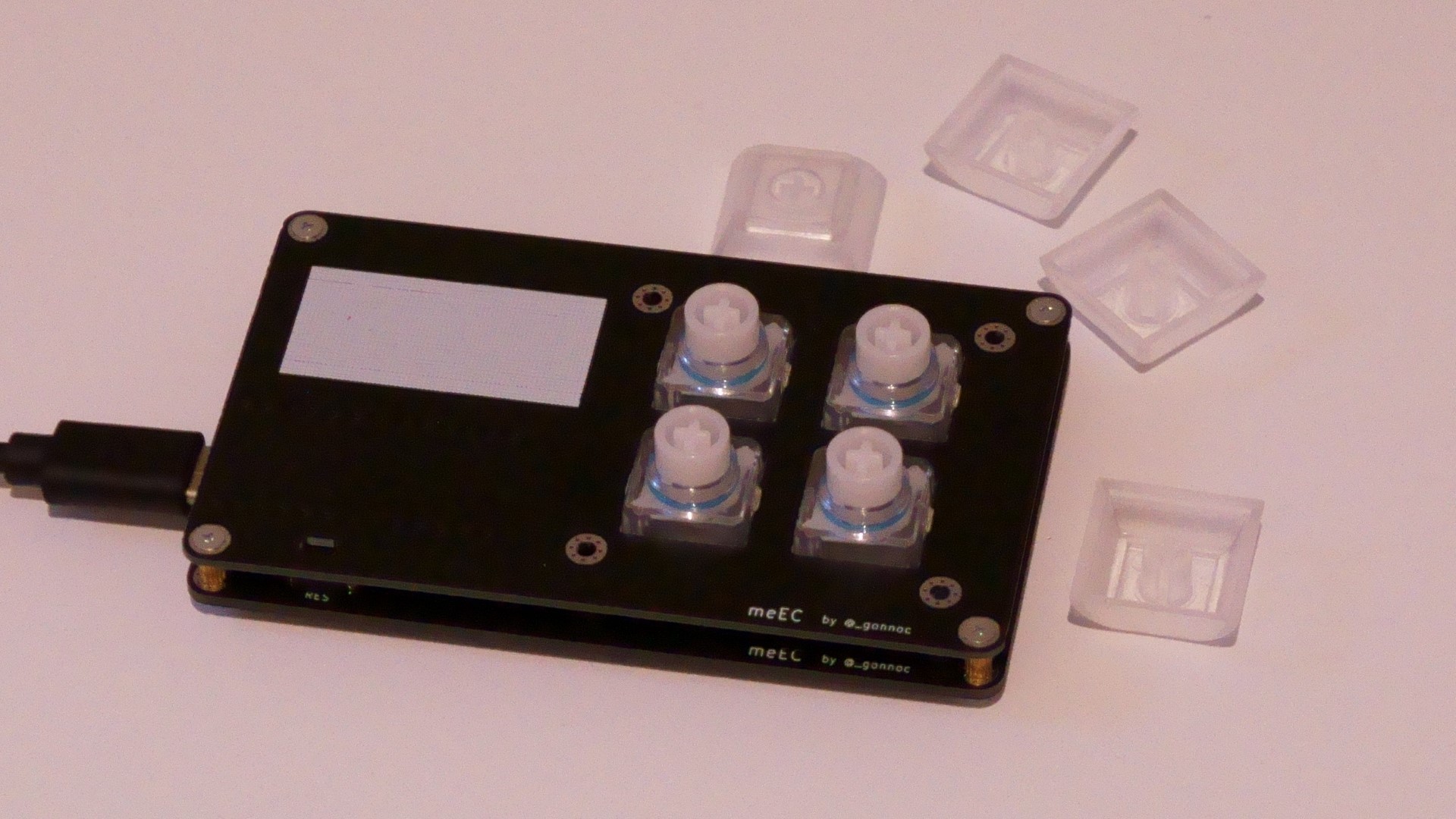 | 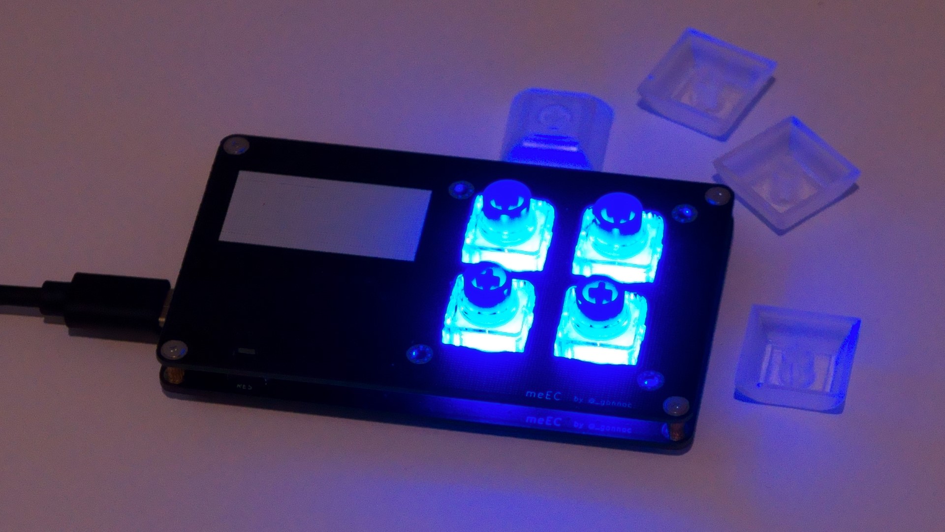 |
|---|---|
| NIZスイッチLEDなし | NIZスイッチLEDあり |
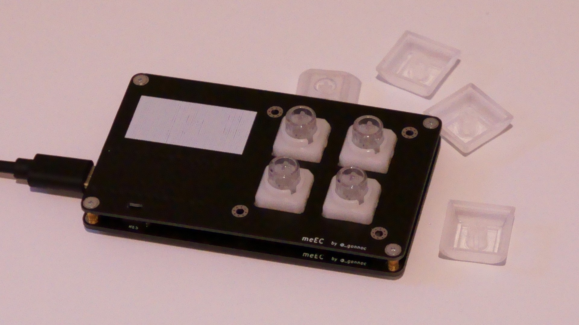 | 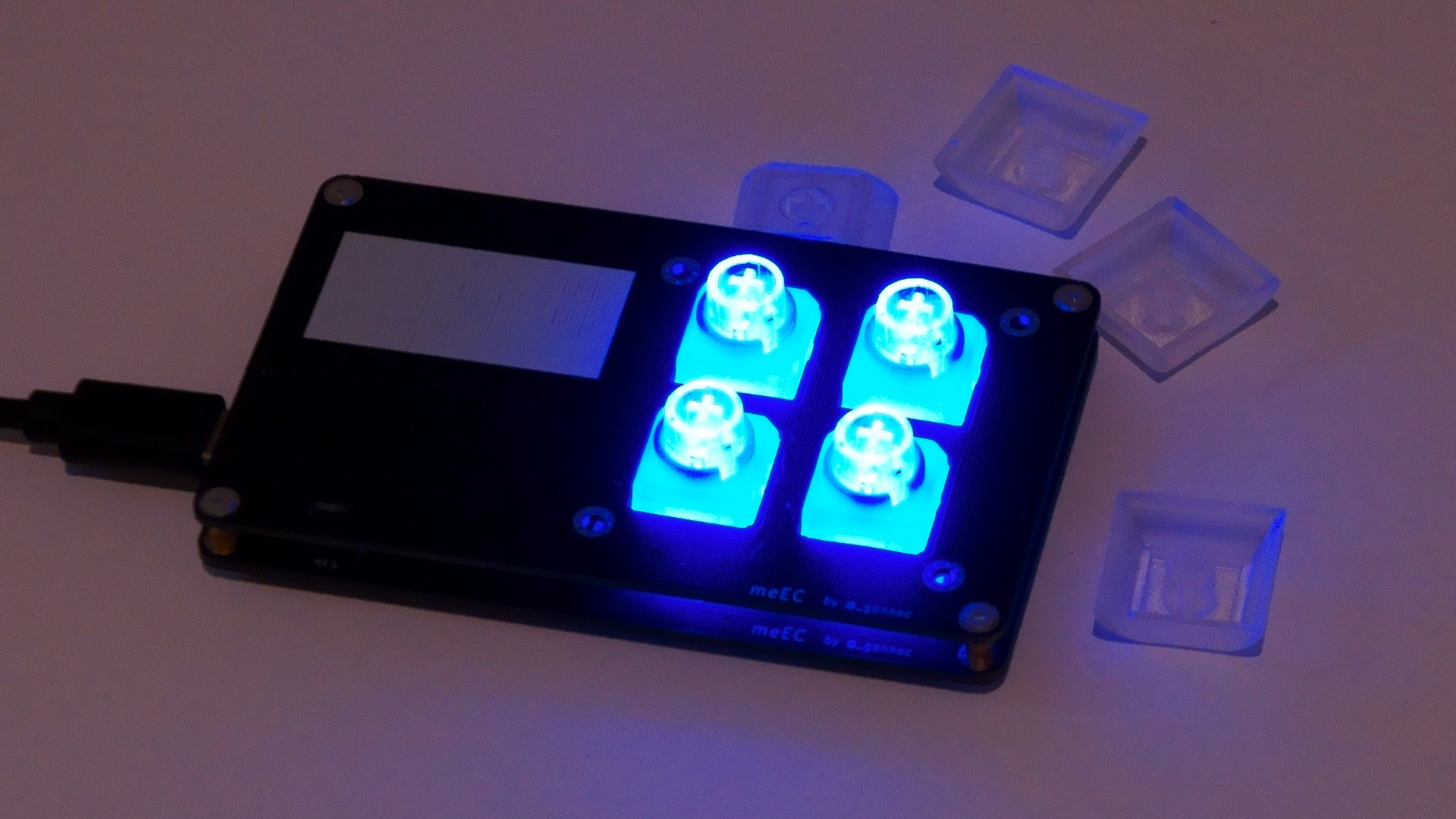 |
| BTOスイッチLEDなし | BTOスイッチLEDあり |
| 部品 | 数 |
|---|---|
| EC micro | 1 |
| USB Type-C コネクタ | 1 |
| メイン基板 | 1 |
| トッププレート | 1 |
| タクトスイッチ | 1 |
| M2ネジ | 8 |
| M2x5スペーサー | 4 |
| ゴム足 | 4 |
| 部品 | 数 | 入手先 |
|---|---|---|
| 12ピンコンスルーまたはピンヘッダ | 2 | 遊舎工房など |
| BTOスイッチ用 | ||
| ADELCPS 静電容量スイッチ4点セット | 4キー分 | https://yushakobo.jp/shop/a0500es-01-1/, https://btoshop.jp/2020/09/25/adelcps/mp |
| ラバードーム | 必要分 | https://yushakobo.jp/shop/a0500er-01-1/, https://btoshop.jp/2020/09/25/adelcpru/ |
| NIZ ECスイッチ用 | ||
| NIZ EC Switch | 4 | https://www.nizkeyboard.com/collections/ornaments/products/2019-new-niz-ec-switch |
| ラバードーム | 必要分 | https://www.nizkeyboard.com/collections/ornaments/products/ec-silicone-domes-35g-45g-55g, 上記ラバードームも可 |
| コニックリング | 4 | NIZ用のバラ売りはないのでBTOのセットなどから流用する |
| LED対応版オプション | ||
| YS-SK6812MINI-E | 4 | 遊舎工房など |
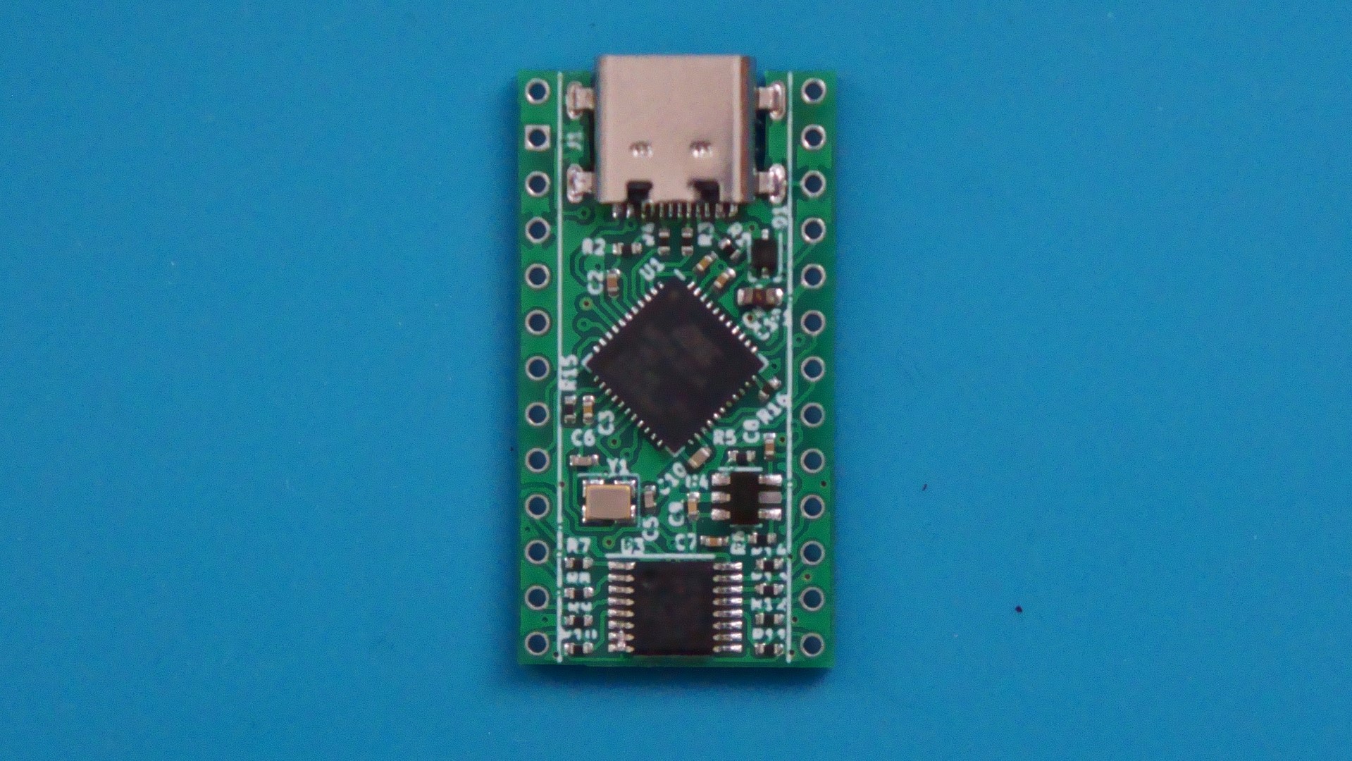
/マークがついている方にLEDの切り欠きを合わせる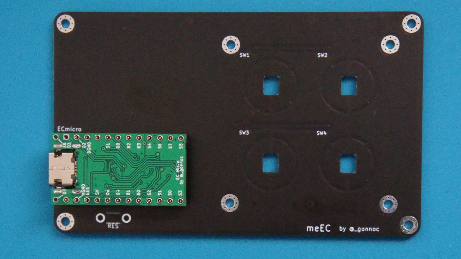
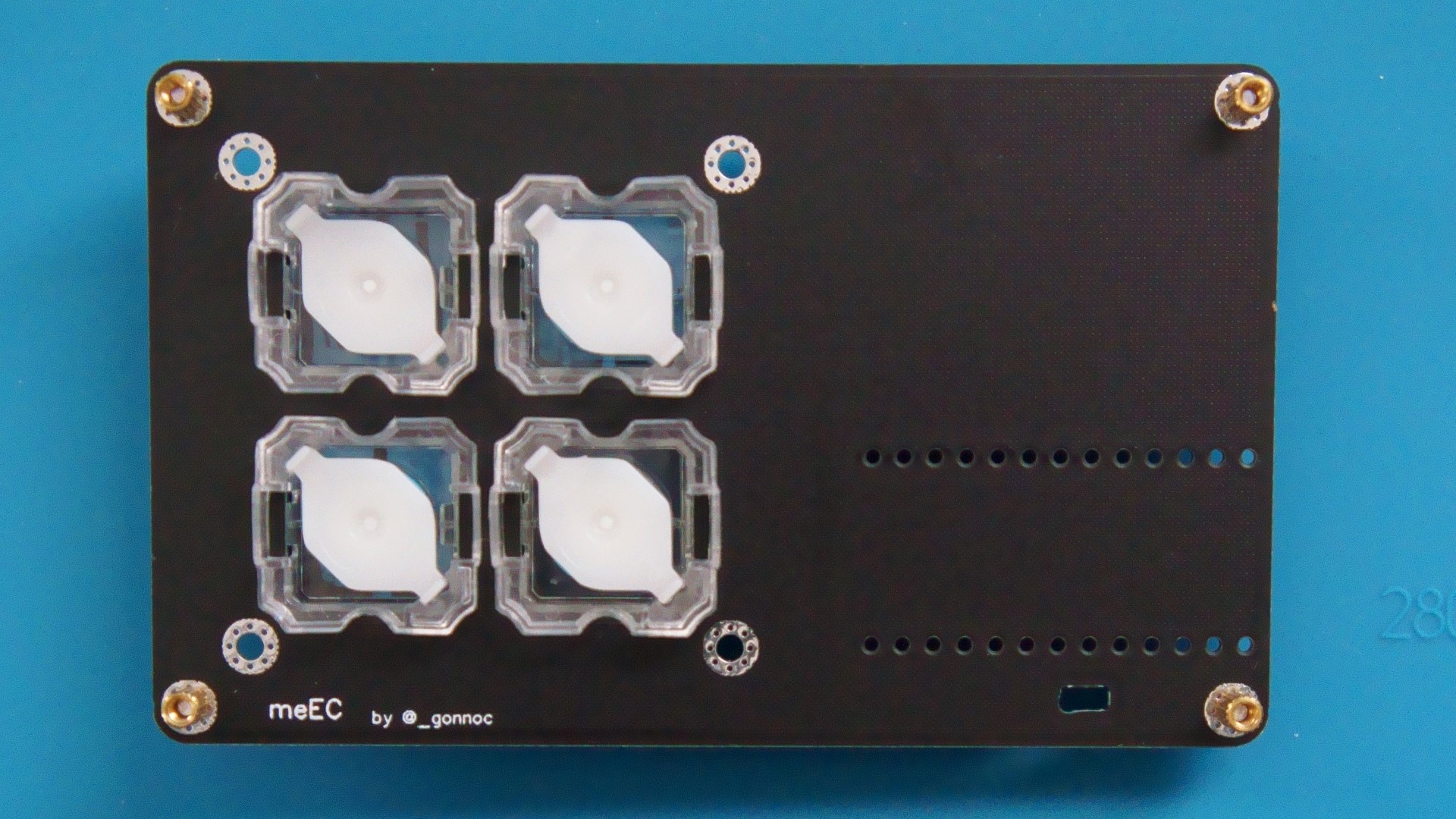
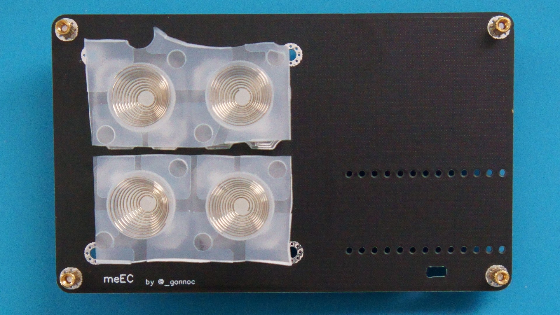
make meec:dfu| Qty | Value | Footprint | References |
|---|---|---|---|
| 8 | M2 | meEC:MountingHole_2.2mm_M2_Pad_Via | H1, H2, H3, H4, H5, H6, H7, H8 |
| 4 | EC_SW | meEC:ec_pad_led2 | SW1, SW2, SW3, SW4 |
| 4 | WS2812B | meEC:YS-SK6812MINI_rev | D1, D2, D3, D4 |
| 1 | ECmicro | meEC:BLEMicroPro | U1 |
| 1 | SW_Push | meEC:TactSW_2Pin | SW5 |
fossasia/pslab-hardware
PSLab Hardware Design and Schematics https://pslab.io

FrameworkComputer/ExpansionCards
Reference designs and documentation to create Expansion Cards for the Framework Laptop


PrintersForAnts/Micron
If you want to purchase full kits there are 3 available (Kits are slowly updating to R1 hardware just make sure to double check the included hardware in your kit and if you have any questions reach out in the discord)


It measures 91 × 55 mm and has 2 copper layers, 1.6 mm thick.
18 parts, built around the WS2812B. The full list of its parts is on this page, with links to each part's symbol and footprint where PCBKit's library has them.
From the sekigon-gonnoc/meEC repository on GitHub, at the commit this page was made from: the board is pcb/meEC.kicad_pcb. PCBKit opens the board in the browser, with nothing to install.
Its repository publishes it under the MIT licence: you may reuse it on that licence's terms (keep the author's notice, and for a copyleft licence share your changes alike).