2 layers100 × 60 mm
 sectersion/loraguide
Hello! In this guide, you will create a custom Meshtastic-enabled LORA board with a microcontroller, antenna, radio chip, and other things.
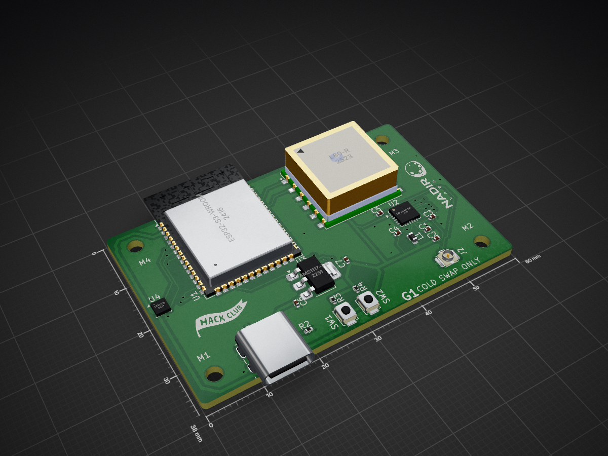
Loraguide is an open-source printed circuit board by sectersion, from the sectersion/loraguide repository on GitHub. It is a 2-layer board of 60 × 38 mm with 27 parts on 57 nets, routed with 227 tracks and 46 vias.
It is built around the ESP32-S3-WROOM-1-N8, L80-R and SX1262IMLTRT, with the BME280 and AMS1117-3.3 among its other parts. Its parts include 7 capacitors, 5 ICs, 4 resistors, 2 connectors and 2 switches. It belongs with the radio and wireless boards and the ESP32 boards of this library.


Hello! In this guide, you will create a custom Meshtastic-enabled LORA board with a microcontroller, antenna, radio chip, and other things.
To start your project, we need to download KiCad. KiCad is an open-source software for designing circuit boards, or PCBs. We can use the terms interchangably.
Go to https://www.kicad.org/download/ and install the version for your OS. After that finishes, create a new project. Name it anything you want, but I will name mine Loraguide.
After that finishes, you should be on a screen that looks like this:
The first step to designing a circuit board is the schematic. A schematic is essentially a wiring diagram, to show which components connect to what. That means it is very important that we follow a few design rules when creating our schematic:
First, click Schematic Editor on the main project page. Hit the A key to open the symbol chooser. Search "esp32-s3" and select the ESP32-S3-WROOM-1.
Place it in the middle. Next, search for the SX1262 radio chip and place it to the left of the ESP32.
To keep things clean, use Power Symbols instead of drawing wires everywhere. Hit P, type +3V3, and place it on the 3V3 pin of the ESP32. Do the same for GND.
Search for "USB_C_Receptacle_USB2.0_14P".
Connect the GND pins to a GND power symbol. Note on the SHIELD pins: Do not connect these directly to GND. This can feed RF noise back into your host computer. For this project, leave the shield pins isolated or connected to a separate chassis pad if available.
Connect VBUS to a +5V power symbol. Place two 5.1k ohm resistors (R_Small) on the CC1 and CC2 pins and connect the other ends to GND. This ensures your USB-C charger provides the correct 5V.
Chips draw sudden bursts of current. Decoupling capacitors (100nF and 10µF) act as local water tanks, sitting right next to the chip to handle these bursts.
Connect VDD_IN to +3V3 and place one 100nF and one 10µF capacitor between that line and GND.
The SX1262 has an internal DC-DC converter that requires a 15µH inductor on the DCC_SW pin. This inductor needs special care; it is a switching component right next to the radio. On the PCB, it must be placed as close as possible to the pin.
Simply running a wire to the antenna is inefficient and can be illegal because it emits harmonics. You need a matching network (filtering) on the RF output. This usually involves a series inductor and capacitors to GND between the RFO pin and the antenna connector.
| Pin | What to do: |
|---|---|
| VDD_IN | Decouple with 100nF and 10µF |
| VBAT | Draw a direct wire to VDD_IN |
| VBAT_IO | Decouple with one 100nF capacitor |
| VREG | Decouple with one 100nF capacitor |
| DCC_SW | Connect 15µH inductor |
| VR_PA | 100nF capacitor to GND (DO NOT connect to 3.3V) |
| GND | Connect directly to GND |
Use an AMS1117-3.3 LDO regulator to convert the 5V from USB to the 3.3V our chips need.
| Pin | Connection |
|---|---|
| VIN | +5V from VBUS + 10µF cap to GND |
| VOUT | +3V3 + 10µF cap to GND |
| GND | GND |
Connect the D+ and D- pins of the USB connector to the USB Data + and - pins on the ESP32. Use Net Labels (L) to keep the wires from crossing.
Both the EN (Reset) and GPIO0 (Boot) pins need a 10kΩ pull-up resistor to 3.3V. Connect push buttons that pull these pins to GND when pressed.
| Signal | ESP32 Pin | SX1262 Pin |
|---|---|---|
| SCK | GPIO5 | SCK |
| MOSI | GPIO6 | MOSI |
| MISO | GPIO7 | MISO |
| NSS | GPIO8 | NSS |
| RESET | GPIO3 | RESET |
| BUSY | GPIO4 | BUSY |
| DIO1 | GPIO9 | DIO1 |
In Tools > Assign Footprints, assign the physical shapes. For resistors and capacitors, R_0402 or C_0402 are standard for these boards.
Sensitive signals must be routed first so they have the cleanest, most direct paths.
Add a Filled Zone (Z) for GND on both the top (F.Cu) and bottom (B.Cu) layers.
To prevent "floating" ground islands and interference, add stitching vias. These are small holes that connect the top and bottom ground planes. Place them around the perimeter of the board and near the RF trace.
Run the DRC (Design Rule Check) to find errors. Export your Gerbers and Drill Files, zip them up, and upload to a manufacturer like JLCPCB.
You have designed a grounded and RF-safe LoRa board.
| Qty | Value | Footprint | References |
|---|---|---|---|
| 4 | 100nF | Capacitor_SMD:C_0402_1005Metric | C1, C3, C4, C5 |
| 4 | MountingHole_2.7mm_M2.5 | MountingHole:MountingHole_2.7mm_M2.5 | M1, M2, M3, M4 |
| 3 | 10uF | Capacitor_SMD:C_0402_1005Metric | C2, C6, C7 |
| 2 | 10k | Resistor_SMD:R_0402_1005Metric | R3, R4 |
| 2 | 5.1k | Resistor_SMD:R_0402_1005Metric | R1, R2 |
| 1 | 15uH | Inductor_SMD:L_0603_1608Metric | L1 |
| 1 | AMS1117-3.3 | Package_TO_SOT_SMD:SOT-223-3_TabPin2 | U3 |
| 1 | BME280 | Package_LGA:Bosch_LGA-8_2.5x2.5mm_P0.65mm_ClockwisePinNumbering | U4 |
| 1 | BOOT | Button_Switch_SMD:SW_SPST_B3U-1000P | SW2 |
| 1 | Conn_Coaxial | Connector_Coaxial:U.FL_Hirose_U.FL-R-SMT-1_Vertical | J2 |
| 1 | ESP32-S3-WROOM-1 | RF_Module:ESP32-S3-WROOM-1 | U1 |
| 1 | L80-R | RF_GPS:Quectel_L80-R | U5 |
| 1 | LOGO | asset_lib:hc_bw_small | G2 |
| 1 | LOGO | asset_lib:nl_bw_large | G1 |
| 1 | RST | Button_Switch_SMD:SW_SPST_B3U-1000P | SW1 |
| 1 | SX1262IMLTRT | Package_DFN_QFN:QFN-24-1EP_4x4mm_P0.5mm_EP2.6x2.6mm | U2 |
| 1 | USB_C_Receptacle_USB2.0_14P | Connector_USB:USB_C_Receptacle_GCT_USB4085 | J1 |
It measures 60 × 38 mm and has 2 copper layers, 1.6 mm thick.
27 parts, built around the ESP32-S3-WROOM-1-N8, L80-R, SX1262IMLTRT and BME280. The full list of its parts is on this page, with links to each part's symbol and footprint where PCBKit's library has them.
From the sectersion/loraguide repository on GitHub, at the commit this page was made from: the board is loraguide.kicad_pcb and its schematic loraguide.kicad_sch. PCBKit opens the board in the browser, with nothing to install.
Its repository states no licence, so its author keeps all rights: ask sectersion before reusing the design.


RichardM-1337/Mesh-Lora-Board
This is a lora board and it's something I've never designed before so I'm attempting something new.

SovietCoffe404/LoRa-Shigihara
This is another HC project, this time is a LoRa board with an ESP32-S3, SX1262 radio, and U.FL antenna! :D

yansha2903-bot/Loraboard
The project was designed using KiCad and includes a complete schematic, PCB layout, and manufacturing files.