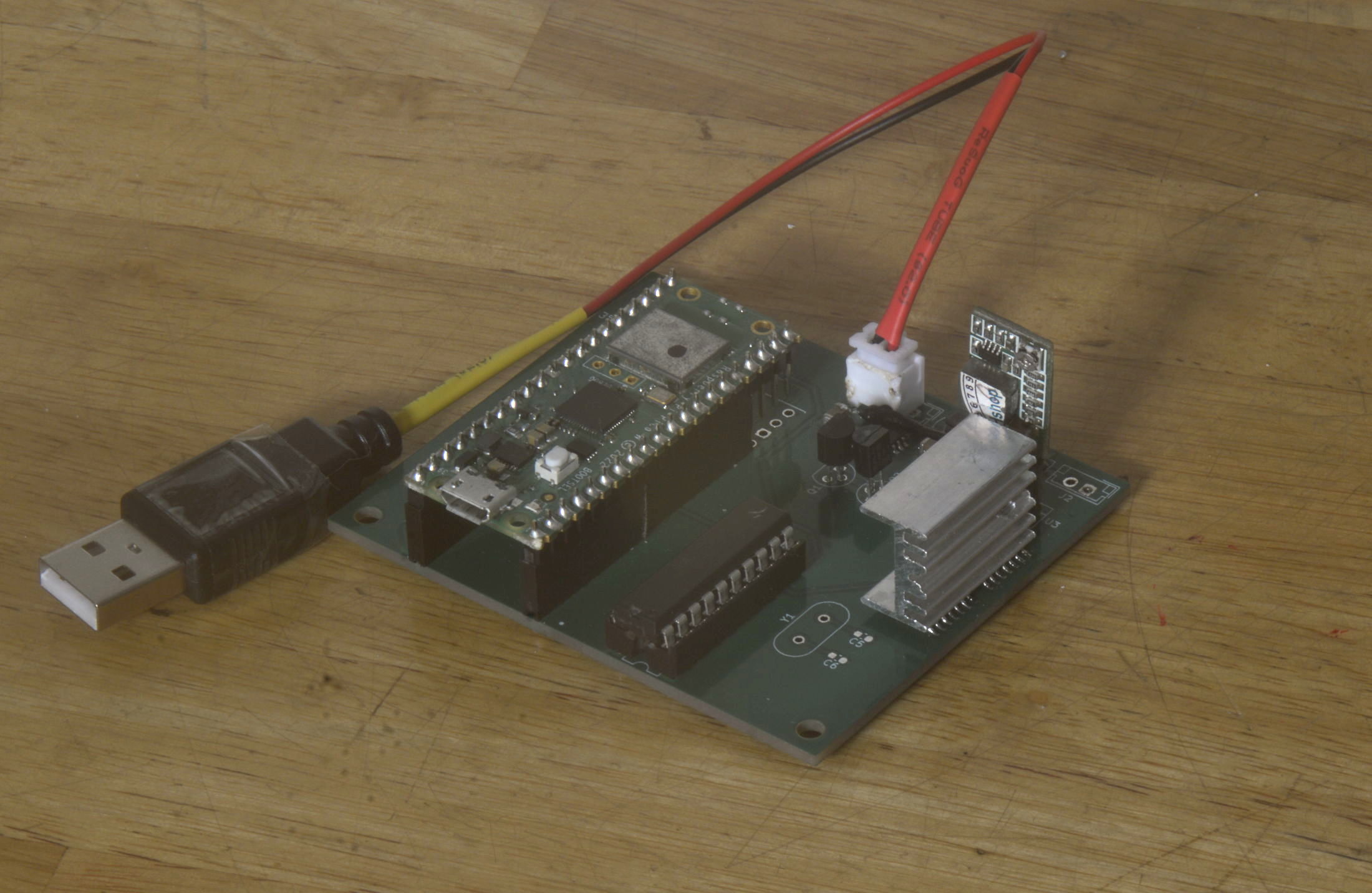
Function
This circuit is designed to output random bytes out MQTT, each as a message. It works at 8-10k bytes per second depending on system voltage and the fact that the bitrate of the entropy source is variable by nature.
What? Why? You could just use a seed phrase and standard cryptography
Yeah, that works fine and there's no real disadvantage.
I've been designing various quantum TRNGs for nearly 15 years as part of an elaborate practical joke. This is just the latest one. I won't tell you what the joke is. Perhaps I'll never tell anyone.
The world could do with a little more whimsy and playful mystery right now, and this is just my little bit that I can share with you.
How it works
The core entropy source is two transistors in an unusual configuration. This is an old technique analogous to the classic "zener diode" method. It has the advantage of producing a slower signal, easier to sample.
It outputs avalanche noise with heavy DC bias. There's some nice summary here.
We remove the DC component wth a capacitor, then use two hex inverters for amplification and pulse-shaping. The first hex inverter is running at ~12V and is configured as two inverting amplifiers -- this is really power inefficient and it gets a bit warm due to the digital part working in linear modes. A little heat sink is recommended.
This unusual use of the hex inverter is to reduce the parts count and cost -- I have a lot of hex inverters lying around. If you needed better power efficiency (e.g. for battery-powered use), you could use an op-amp. OPA132 is pretty easy to use.
The next hex inverter operates more or less digitally, just shaping the signal into a clean square wave. This one does not get warm.
After that, an Attiny261A acts as a Von Neumann extractor to convert the square wave into usable, unbiased bits of entropy.
The bytes are read by a Pi Pico W and pushed out MQTT. Basic authentication works. I didn't bother adding TLS.
It would be possible to just use the PIO of the Pi Pico instead of an Attiny261A. However, most of the time I don't actually want the Pi Pico or Wi-Fi, and am just using the entropy locally. If you wanted to do this, you would simply not populate the Attiny261A, and solder a wire between pin 9 of the Attiny socket, and whatever pin you want on the Pi Pico. That will bypass the Attiny261A and push the raw entropy signal directly to the Pi Pico. I would recommend writing your own Von Neumann extractor with the PIO.
How to build it
Notes on surface mount components
This design makes extensive use of surface-mount components. I have limited budget and time to spend on my hobbies, so I generally use the smallest possible SMT components to save both (standardize my parts library). If you find 0402 difficult to work with, then it's very fast to open up the KiCAD files in this repo, and replace all the 0402 resistors with 0603 in the schematic. Then just pull up the board design, update from the schematic, and touch up the routing -- you should be good to go, 0603 is pretty easy to hand-solder even without a hot air rework station and solder paste. A normal iron, coil of solder, and some patience will suffice.
If you want to redesign everything as through-hole, this will require a bit of a redesign. I would recommend purchasing a USB boost converter, not populating the integrated boost converter, and using the passthrough I've left you (J2). Then switch the CD4069 to the DIP version, and add in through-hole resistors and capacitors. I vaguely recall that the DIP version of the CD4069 has better thermal dissipation, you might be able to get away with a smaller heat sink or none at all -- I've gotten away without one in older designs (give it a careful test though).
Building the current design
I recommend building the boost converter first, then give it some power and make sure the output voltage is sane. Should be between 12 and 13 volts. Note that the EN pin of the MT3608 should be connected to Vin -- else nothing will output at all. I just bridge the middle pin of J1 to Vin.
Once that's in, I put in the transistors (mind polarity!), the first hex inverter, and all the resistors and capacitors around them. Then I supply power again, for a short time, with a scope connected to the output of the first hex inverter. The scope is set to be AC coupled. I should see a pretty looking signal with a lot of noise. Then I cut power -- that first hex inverter can get sort of hot with no heat sink attached.
Then I get the buck converter / LM7803 in, as well as the final hex inverter. Then I test as above (scope can be AC or DC coupled), making sure the signal from the second hex inverter is a weird looking, but mostly clean square wave ranging from 0 to 3.3V.
If that's good, I flash the program (main.asm) to an Attiny261A (using AVR-ICE, STK500 or home-made programmer). For the first few boards, I put in a socket for the AVR, so I can pull it out and update the firmware. Then I quickly check again, specifically that the "new output" pin of the Attiny261A is pushing out 10 usec pusles, and that bits are coming out of the pins of PORTA.
At this point, I just load the program (main.py) into the Pi Pico, disconnect it from the USB cable, and plug it in. The onboard LED should light up if it's receiving power, and flicker slightly if it's pushing out MQTT. If it doesn't flicker, try turning it off and on again, sometimes it can fail to connect to Wi-Fi.
DO NOT plug a USB cable into the Pi Pico while it is connected to this circuit It is being powered by 3.3V. USB is 5V. Several components are likely to make sad electronic noises, fail violently, and lose their magic blue smoke.
As for what part goes where? It's all in the KiCAD schematic. I would recommend giving it a detailed look.
The Von Neumann Extractor
This just measures two time intervals between 2 sets of 2 independent events (it could probably use 3 events instead of 4 to calculate 2 intervals, but whatever. It's much faster than fast enough now). If t1>t2, it records a 0. If t1<t2, it records a 1. If they are equal, it tries again.
I originally wrote this firmware ages ago. It was quite an experience to look at my ham-fisted assembly from 15 years ago. I redid it with many optimizations, which increased performance about 50x. Also it consumes less power. Use main.asm, not old_von_neumann.asm. Seriously, the latter is pretty awful.
I include both files, so that one day I may look back and consider both attempts primitive and silly. Got to keep that ego in check!
Photo
Note the black "bodge wire" near the USB power input. This was necessary because of an error in the original design files. The version in this repository has been corrected, and you won't need to cut any traces / add weird wires and so on.