4 layers227 × 40 mm

 scrambletools/ES8389-Hat
Hat for Waveshare ESP32-P4-ETH and Raspberry Pi Pico
Scramble hat is an open-source printed circuit board by scrambletools, from the scrambletools/ES8389-Hat repository on GitHub. It is a 4-layer board of 51.4 × 21.1 mm with 79 parts on 62 nets, routed with 1,069 tracks and 138 vias.
It is built around the ES8389, 74HC4053D and TPS7A2033DQN, with the KAQY214S, NCJ6FA-H and SS-12D00-G3 among its other parts. Its parts include 29 capacitors, 26 resistors, 7 connectors, 6 diodes and 4 ICs.


A compact 4-layer audio I/O HAT that stacks on a Waveshare ESP32-P4 carrier and gives it a studio-style balanced input and a headset/line output, bridged to the host over I²S (audio) and I²C (control). Its headline trick: it taps the carrier's 802.3 PoE rail to generate switchable ~48 V-class phantom power for condenser microphones — no separate supply.
Target carrier: a Waveshare ESP32-P4-ETH board with PoE module. You will need to solder taps on the output of the bridge rectifiers of the PoE module and connect those wires to J5 on the hat.
  XLR / 6.35" combo (J1) ──coupling──▶ ES8389 ADC ──▶ I²S ──▶ ESP32-P4 carrier
         ▲ phantom
  PoE (J5) ─F1─▶ SW1 ─opto OK1─▶ P-FET Q1 ─▶ 6.81k feed ─▶ XLR pins 2 & 3

  ESP32-P4 carrier ──▶ I²S ──▶ ES8389 DAC ──coupling──▶ TRRS out (J2)
ESP32-P4 carrier ◀──▶ I²C ◀──▶ ES8389 (+ external display header J6)| Ref | Part | Function |
|---|---|---|
| J1 | Neutrik NCJ6FA-H | XLR / ¼″ combo — balanced mic/line input; ¼″ side is a Hi-Z instrument input with auto-detect (hand-solder) |
| J2 | CUI SJ-3524 TRRS | 3.5 mm headset — stereo output + electret mic (hand-solder) |
| J3, J4 | 1×7 sockets (8.5 mm) | mezzanine to the carrier — I²S, I²C, power |
| J5 | 1×2 header | PoE rail input from the carrier's PoE module (hand-solder) |
| J6 | 1×4 header | external I²C display (3V3 / GND / SDA / SCL) — DNP; hand-fit (top side) only for a display harness. Eurorack builds don't need it: the interposer drives the display directly |
| SW1 | SPDT slide | phantom power on/off (manual) — DNP; populate only in builds that use phantom. Unpopulated = phantom permanently off; for switchless always-on phantom, bridge SW1 pads 1–2 instead |
| Ref | Part | Role |
|---|---|---|
| U1 | Everest ES8389 (QFN-24) | stereo audio codec |
| U2 | TI TPS7A2033 | ultra-low-noise 3.3 V analog LDO |
| OK1 | Everlight EL3H7 (80 V) | opto-isolated phantom enable |
| Q1 | Vishay Si2325DS | P-FET phantom high-side switch |
| F1 | 100 mA / 60 V PPTC | phantom / PoE overcurrent protection |
| D6 | SMBJ58CA TVS | PoE-rail clamp |
| D8 | white LED | phantom-present indicator |
| C19 | 2.2 nF Y2 | isolation-barrier safety cap |
The codec carries audio over I²S and is controlled over I²C. Its I²C address is set by the AD0/AD1 straps (R3/R4); R1/R2 are the SDA/SCL pull-ups. Typical firmware is ESPHome or ESP-ADF configured for an external I²S codec.
The header assignment is chosen so one unmodified board works on two hosts: the Waveshare ESP32-P4-ETH carrier it was designed for, and a Raspberry Pi Pico — the hat's footprint (2.54 mm pitch, ~17.8 mm row spacing, 51 × 21 mm outline) lands exactly on the Pico's USB-end pins 1–7 / 40–34.
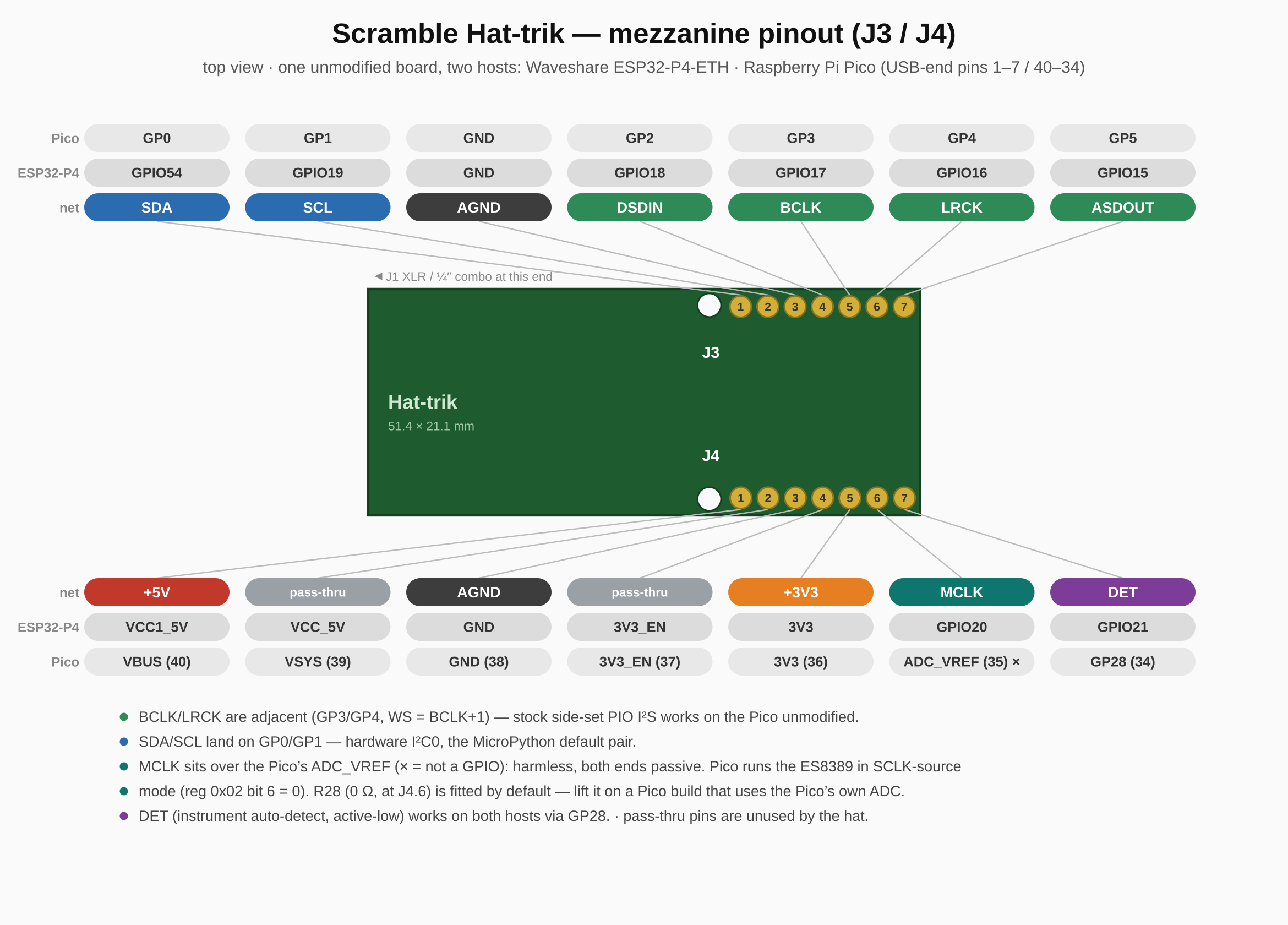
| J3 pad | net | P4-ETH | Pico | J4 pad | net | P4-ETH | Pico | |
|---|---|---|---|---|---|---|---|---|
| 1 | SDA | GPIO54 | GP0 | 1 | +5V | VCC1_5V | VBUS | |
| 2 | SCL | GPIO19 | GP1 | 2 | pass | VCC_5V | VSYS | |
| 3 | AGND | GND | GND | 3 | AGND | GND | GND | |
| 4 | DSDIN | GPIO18 | GP2 | 4 | pass | 3V3_EN | 3V3_EN | |
| 5 | BCLK | GPIO17 | GP3 | 5 | +3V3 | 3V3 | 3V3(OUT) | |
| 6 | LRCK | GPIO16 | GP4 | 6 | MCLK | GPIO20 | ADC_VREF — unused | |
| 7 | ASDOUT | GPIO15 | GP5 | 7 | DET | GPIO21 | GP28 |
Why it lands this way:
Pico caveats: +5V is VBUS, so the analog LDO only runs on USB power;
phantom power is unavailable (no PoE front end — see the phantom
section below); full-duplex I²S needs a custom PIO RX machine against
the TX clocks; no ES8389 driver exists for the Pico yet (port from
ESP-ADF or the mainline Linux es8389.c). For low BCLK jitter set
sys_clk to 153.6 MHz so 3.072 MHz divides exactly.
Phantom power is the one hat feature that needs more than the mezzanine:
the 48 V-class rail is tapped from the PoE bus and enters the hat on
J5 (pin 1 = TAP_HV +, pin 2 = TAP_GND −). On the ESP32-P4-ETH
carrier, the RJ45 mag-jack's pair centre taps run raw to the H7 header;
the plug-in PoE module on H7 carries the bridge rectifiers (BD1/BD2)
that turn them into 37–57 V DC before its isolated DC-DC makes the 5 V.
Tap the two bridge-rectifier outputs on the PoE module — + to
J5.1, − to J5.2. The module has no connector for the tap, so the
two leads are hand-soldered directly to the rectifier output pins; keep
them reasonably short:
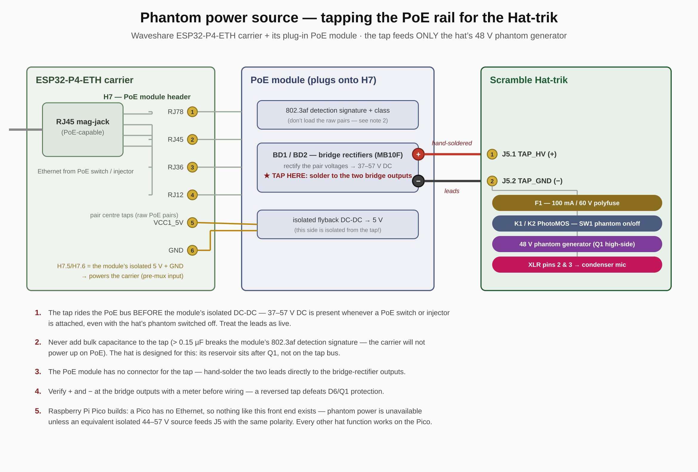
+/− with a meter at the bridge outputs before wiring; a
reversed tap defeats the D6/Q1 protection.Two validated configurations, using the AVB endpoint firmware's controls
(ES8389 PGA via the entity's Mic Gain control; digital gain via the talker's
ESP_AVB_TALKER_MIC_DIGITAL_GAIN_DB Kconfig, which also engages an always-on
DC-block ahead of the gain):
| Condenser (phantom) | Dynamic | |
|---|---|---|
| Phantom switch (SW1) | ON | OFF |
| PoE feed (J5) | connected + powered | disconnect the PoE module (see note) |
| ES8389 PGA gain | +36 dB | +36 dB (ceiling is +36.5 dB) |
| Digital gain (Kconfig) | 0 dB | +20 dB |
Notes:
The ¼″ side of J1 feeds a high-impedance buffer (U3, ~500 kΩ input) into the
codec's MIC1 channel through an analog mux (U4). Inserting a mono TS plug
(guitar cable) shorts the jack's Ring contact to the Sleeve, pulling the
DET line low — this automatically switches MIC1 from the XLR mic path to
the buffered instrument path, and is readable by the carrier on J4.7
(input, active-low = instrument present). Remove the plug (or use an XLR
mic) and the input returns to the mic path. Phantom power never reaches the
¼″ contacts.
Hardwiring a guitar without installing the Neutrik connector — three connections on the J1 footprint, not two:
| Guitar wire | Pad | Note |
|---|---|---|
| Tip (signal) | either T pad | the two T holes are the same net (GTIP); one is enough |
| Sleeve (ground) | S pad | PGND; the larger G pad is the same net if a thicker wire is used |
| — | jumper R → S | required. With no jack fitted, nothing shorts Ring to Sleeve, so DET stays high and the mux stays on the (absent) XLR path — the guitar would be silent. The jumper forces instrument mode. Easiest form: populate R27 (0805 0 Ω, DNP by default) — it shorts DET to PGND on-board. Remove/leave it off if the Neutrik is fitted. |
Eurorack module link (J7): instead of hand-wiring, an optional 1×4
female socket J7 (8.5 mm stacking, same series as J3/J4, DNP by
default) direct-mates the Synthia eurorack interposer's J8 header. Populate J7
only when J1 is absent (they use the same input path), and populate
R27 with it (the module's input jack can't pull DET low). Pinout:
1 = GTIP, 2 = PGND, 3 = AGND, 4 = HP_L_OUT — signals on the outer
pins with both grounds between them.
Eurorack + display: the interposer drives a display directly from its own display socket (J10, on the main GND/3V3/I²C nets), so J6 can stay DNP in eurorack builds — no bottom-side fitting needed. Fit J6 (top side) only for a normal display harness in non-rack builds.
Cable: use two-core shielded cable (the input is high impedance and hums otherwise) — one core to T (signal), the other core to S (return), and the shield joined to S at the hat end only; at the guitar end connect just the two cores (tip / sleeve) and trim + insulate the shield. The return current then flows in the tightly-coupled core pair while the shield does pure screening — bonding it at both ends would let ground-loop and pickup currents flow through it in series with the signal. For very short runs (a few cm) plain coax — center to T, shield as the return to S, connected at both ends — also works.
To feed a mono amplifier that expects only tip and sleeve, skip the 3.5 mm jack
and solder wires directly to the J2 footprint. Careful: J2 is wired as a
CTIA TRRS headset jack, so the pad named S is not ground — on CTIA the
physical sleeve is the microphone conductor.
| Amp wire | Pad | Note |
|---|---|---|
| Tip (signal) | T | HP_L_OUT — left audio channel |
| Sleeve (ground) | TN | AGND — audio ground. Do not use the S pad: it is the headset-mic line (MIC2_RAW) and carries mic bias — grounding it gives hum and injects into the MIC2 input. |
Notes:
T and R pads to "sum" the
channels — that shorts the two DAC output stages into each other. (A passive
sum, if ever wanted, is a ~1 kΩ resistor from each of T and R into the amp
tip.)| Path | Contents |
|---|---|
scramble_hat.kicad_sch / .kicad_pcb | hierarchical schematic + layout |
BOM.csv | bill of materials — single source of truth |
fab/ | JLCPCB gerbers, drills, BOM, CPL — see fab/README.md |
tools/gen_fab.py | regenerate every production file from the design |
tools/check_sync.py | verify schematic ↔ PCB netlist agreement |
lib/ | project symbols, footprints, 3D models |
docs/ | schematic + silkscreen PDFs |
See fab/README.md for the full ordering guide. In short: JLCPCB
fabricates and assembles most parts; you hand-solder J1, J2, J5 and C19 (the Y-cap),
and R14 is left unpopulated (DNP ground-lift jumper). J6 (display header) is also
DNP — hand-fit it only when a display is used (top side normally, bottom side for the
eurorack stack). Regenerate all fab outputs with:
python3 tools/gen_fab.py⚠️ Before committing an assembly order, verify part rotations in JLCPCB's preview — especially U1 (the QFN's rotation is applied manually and is a best estimate).
| Qty | Value | Footprint | References |
|---|---|---|---|
| 12 | 1uF | Capacitor_SMD:C_0402_1005Metric | C2, C5, C7, C8, C9, C12, C20, C21, C23, C24, C25, C26 |
| 6 | 100nF | Capacitor_SMD:C_0402_1005Metric | C1, C3, C4, C27, C28, C29 |
| 5 | 100k | Resistor_SMD:R_0402_1005Metric | R11, R13, R19, R22, R23 |
| 3 | 10k | Resistor_SMD:R_0402_1005Metric | R1, R2, R25 |
| 3 | 33R | Resistor_SMD:R_0402_1005Metric | R9, R10, R24 |
| 2 | 1M | Resistor_SMD:R_0402_1005Metric | R21, R26 |
| 2 | 1uF | Capacitor_SMD:C_0805_2012Metric | C10, C11 |
| 2 | 22uF | Capacitor_SMD:C_0805_2012Metric | C14, C15 |
| 2 | 470 | Resistor_SMD:R_0402_1005Metric | R17, R18 |
| 2 | 6.81k 1% | Resistor_SMD:R_0805_2012Metric | R5, R6 |
| 2 | KAQY214S | Package_SO:SOP-4_3.8x4.1mm_P2.54mm | K1, K2 |
| 2 | PESD3V3L1BA (ESD) | Diode_SMD:D_SOD-323 | D1, D2 |
| 1 | 0R (MCLK link) | Resistor_SMD:R_0805_2012Metric | R28 |
| 1 | 0R DNP (PGND lift) | Resistor_SMD:R_0402_1005Metric | R14 |
| 1 | 100nF 100V | Capacitor_SMD:C_0805_2012Metric | C30 |
| 1 | 100nF/100V | Capacitor_SMD:C_0805_2012Metric | C17 |
| 1 | 10k (AD0 strap) | Resistor_SMD:R_0402_1005Metric | R3 |
| 1 | 10k (AD1 strap) | Resistor_SMD:R_0402_1005Metric | R4 |
| 1 | 10uF | Capacitor_SMD:C_0805_2012Metric | C6 |
| 1 | 15k | Resistor_SMD:R_0805_2012Metric | R16 |
| 1 | 1k | Resistor_SMD:R_0402_1005Metric | R12 |
| 1 | 1uF (bias filter) | Capacitor_SMD:C_0402_1005Metric | C13 |
| 1 | 1uF/100V | Capacitor_SMD:C_1206_3216Metric | C18 |
| 1 | 2.2k | Resistor_SMD:R_0402_1005Metric | R20 |
| 1 | 2.2k (mic bias) | Resistor_SMD:R_0402_1005Metric | R7 |
| 1 | 2.2nF Y2 (PGND-AGND) | scramble_hat:C_Y2_DE2B_TH | C19 |
| 1 | 2.2uF | Capacitor_SMD:C_0402_1005Metric | C22 |
| 1 | 600R@100MHz | Inductor_SMD:L_0603_1608Metric | FB1 |
| 1 | 74HC4053 | Package_SO:TSSOP-16_4.4x5mm_P0.65mm | U4 |
| 1 | Carrier LEFT 1-7 | Connector_PinSocket_2.54mm:PinSocket_1x07_P2.54mm_Vertical | J3 |
| 1 | Carrier RIGHT 1-7 | Connector_PinSocket_2.54mm:PinSocket_1x07_P2.54mm_Vertical | J4 |
| 1 | DMP3098 (P-FET 60V) | Package_TO_SOT_SMD:SOT-23 | Q1 |
| 1 | ES8389 | scramble_hat:ES8389_QFN24_P0.35mm | U1 |
| 1 | I2C 3V3/AGND/SDA/SCL | Connector_PinHeader_2.54mm:PinHeader_1x04_P2.54mm_Vertical | J6 |
| 1 | LED white 0805 | LED_SMD:LED_0805_2012Metric | D8 |
| 1 | MMSZ4699 (Zener 12V) | Diode_SMD:D_SOD-123 | D7 |
| 1 | NCJ6FA-H | Connector_Audio:Jack_XLR-6.35mm_Neutrik_NCJ6FA-H_Horizontal | J1 |
| 1 | Polyfuse 50mA | Fuse:Fuse_1812_4532Metric | F1 |
| 1 | R0 (force instrument mode) | Resistor_SMD:R_0805_2012Metric | R27 |
| 1 | SMBJ58CA (TVS 58V) | Diode_SMD:D_SMA | D6 |
| 1 | SS-12D00-G3 | scramble_hat:SW_Slide_SS-12D00-G3 | SW1 |
| 1 | TLP291 | Package_SO:SOP-4_4.4x2.6mm_P1.27mm | OK1 |
| 1 | TLV9061 | Package_TO_SOT_SMD:SOT-23-5 | U3 |
| 1 | TO EURORACK MODULE (alt. to J1) | Connector_PinSocket_2.54mm:PinSocket_1x04_P2.54mm_Vertical | J7 |
| 1 | TPD1E10B06 (ESD) | Package_SON:Texas_DPY0002A_0.6x1mm_P0.65mm | D9 |
| 1 | TPS7A2033 | Package_TO_SOT_SMD:SOT-23-5 | U2 |
| 1 | TRRS PJ-3X4S (CTIA, bottom-side) | Connector_Audio:Jack_3.5mm_CUI_SJ-3524-SMT_Horizontal | J2 |
| 1 | VDD_PoE / PGND | Connector_PinHeader_2.54mm:PinHeader_1x02_P2.54mm_Vertical | J5 |

PKCubed/RJ45XLR
A simple, robust PCB that allows a shielded twisted pair category cable (Cat5e, Cat6a, etc.) to take the place of up to four heavy XLR cables.

crsknr/hw_udsp-card
A compact DSP development board for real-time embedded audio and sensing

Phalkon-Industries/phoenix-instrument
Git repo for the content of the new Phoenix ph handheld instrument.

8aChristian/BIOCHEST-ECG-EMG
Figure 1: Full 4-Layer High-Density Medical PCBA with Galvanic Isolation Barrier & Routed Copper Tracks.

aswinserigreen/morishield_hardware
all components bom , pcb layouts and schematics of morishield is maintained here

botsqerebot/AudioDeck
Everything to change, check and test for rev 2. The main goal is power saving while the player is off:

It measures 51.4 × 21.1 mm and has 4 copper layers, 1.6 mm thick.
79 parts, built around the ES8389, 74HC4053D, TPS7A2033DQN and KAQY214S. The full list of its parts is on this page, with links to each part's symbol and footprint where PCBKit's library has them.
From the scrambletools/ES8389-Hat repository on GitHub, at the commit this page was made from: the board is scramble_hat.kicad_pcb and its schematic scramble_hat.kicad_sch. PCBKit opens the board in the browser, with nothing to install.
Its repository states no licence, so its author keeps all rights: ask scrambletools before reusing the design.