Skip to the content
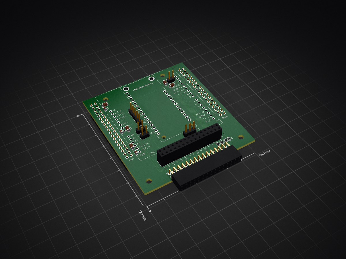
2 layers69.7 × 77.1 mmExperimental Kit, the printed circuit board in 3D

Experimental Kit

sckim/KiCAD

휘트스톤 브리지(Wheatstone Bridge)는 저항 4개로 두 개의 분압기를 만들고, 두 중간점의 전압 차이로 저항의 균형 여부를 판단하는 회로이다. 이 예제에서는 예제 1의 흐름(회로도 → PCB)에 더해 KiCad에 내장된 SPICE 시뮬레이터(ngspice) 로 회로를 먼저 계산해 보는 방법을 익힌다.

Size
69.7 × 77.1 mm
Copper layers
2
Thickness
1.6 mm
Parts
27
Nets
95
Pads
242
Tracks, vias
428, 16
Routed
Yes
KiCad
KiCad 10.0 (file 20260206)
Created
7 Jan 2025
Updated
25 Sep 2026

Overview

Experimental Kit is an open-source printed circuit board by sckim, from the sckim/KiCAD repository on GitHub, published under the GPL-3.0 licence. It is a 2-layer board of 69.7 × 77.1 mm with 27 parts on 95 nets, routed with 428 tracks and 16 vias.

It is built around the ARDUINO UNO R3. Its parts include 9 connectors, 8 capacitors and 4 resistors. It belongs with the AVR (ATmega, ATtiny) boards of this library.

Main components

1

README

20_WheatstoneBridge/README.md

예제 2. Wheatstone Bridge — 회로 시뮬레이션과 PCB

휘트스톤 브리지(Wheatstone Bridge)는 저항 4개로 두 개의 분압기를 만들고, 두 중간점의 전압 차이로 저항의 균형 여부를 판단하는 회로이다. 이 예제에서는 예제 1의 흐름(회로도 → PCB)에 더해 KiCad에 내장된 SPICE 시뮬레이터(ngspice) 로 회로를 먼저 계산해 보는 방법을 익힌다.

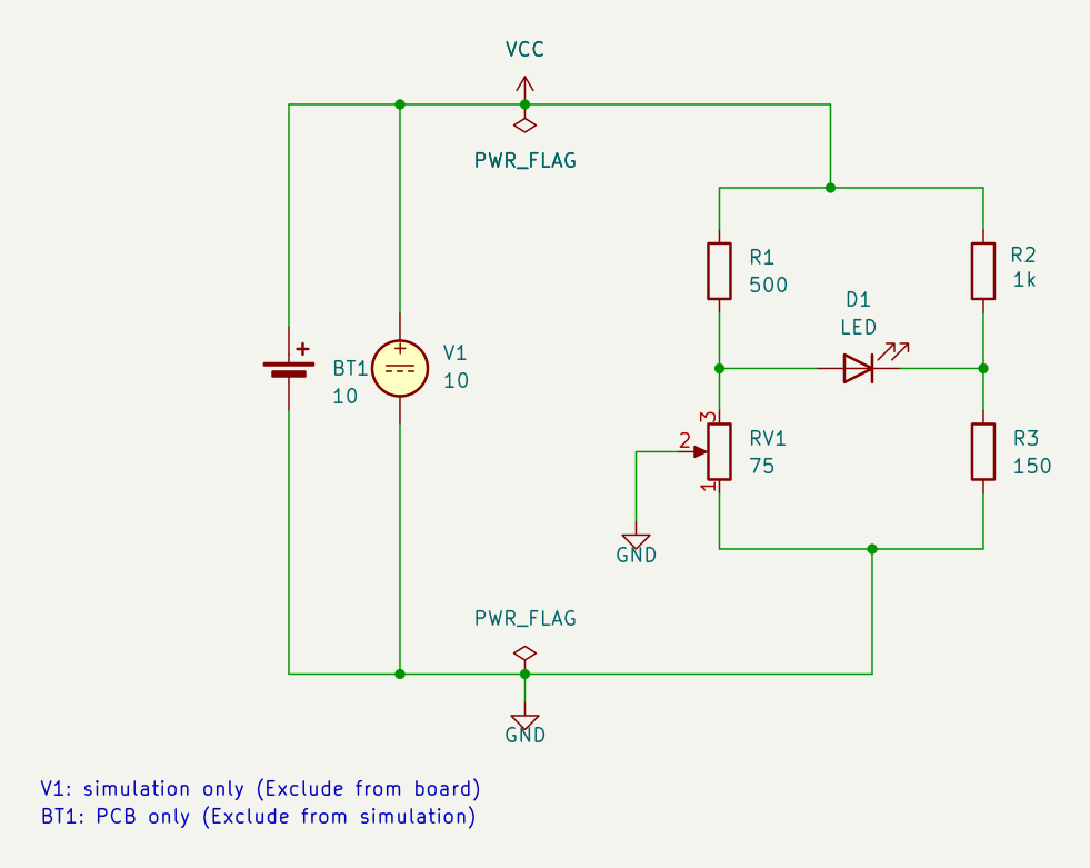
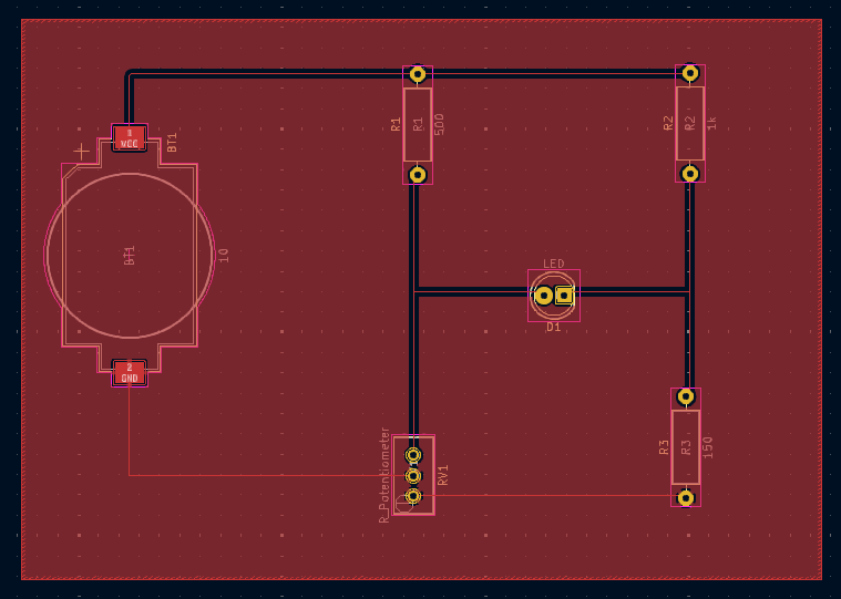
Wheatstone Bridge 회로도Wheatstone Bridge PCB

이 예제는 예제 1을 마쳤다고 가정한다. 회로도 그리기, 풋프린트 지정, PCB 배선 방법은 예제 1을 참고한다.


1. 폴더 구성

파일설명
WheatstoneBridge.kicad_pro프로젝트 파일이다. 이 파일을 연다.
WheatstoneBridge.kicad_sch회로도 (시뮬레이션 설정 포함)
WheatstoneBridge.wbk시뮬레이터 작업 파일(workbook)이다. 해석 종류와 명령이 저장되어 있다.
WheatstoneBridge.kicad_pcbPCB 레이아웃
gerber/PCB 제작 파일(거버, 드릴)

2. 회로 이해하기

전원(10 V)과 GND 사이에 분압기 두 개가 나란히 연결되어 있다.

text
         VCC (10 V)
        ┌────┴────┐
        R1 500Ω   R2 1kΩ
        │         │
  A ────┤         ├──── B
        │   D1    │
        │ A ▶|─ K │          A: LED 애노드 쪽, B: LED 캐소드 쪽
        │         │
       RV1 75Ω   R3 150Ω
        └────┬────┘
            GND
참조 번호부품값역할
V1DC 전압원 (Simulation_SPICE:VDC)10 V시뮬레이션 전용 전원 (Exclude from board)
BT1전지 (Device:Battery_Cell)—PCB 전용 전원 (Exclude from simulation)
R1, RV1저항, 가변저항(트리머)500 Ω, 75 Ω왼쪽 분압기 → 점 A
R2, R3저항1 kΩ, 150 Ω오른쪽 분압기 → 점 B
D1LED (Device:LED) + 다이오드 모델—A와 B 사이 전압 차 검출. 시뮬레이션과 PCB에 모두 쓰인다

브리지 평형 조건

두 분압기의 비율이 같으면 A와 B의 전압이 같아지고 LED에는 전류가 흐르지 않는다. 이를 평형(balanced) 상태라고 한다.

text
R1 / RV1 = R2 / R3   →   RV1 = R1 × R3 / R2 = 500 × 150 / 1000 = 75 Ω

손으로 계산한 각 점의 전압은 다음과 같다.

text
V_B = 10 V × R3 / (R2 + R3)   = 10 × 150 / 1150 ≈ 1.30 V   (고정)
V_A = 10 V × RV1 / (R1 + RV1)                                (RV1에 따라 변함)
RV1 posA–GND 사이 저항V_AV_A − V_B상태
075 Ω1.30 V0 V평형
0.537.5 Ω0.70 V−0.61 V불평형 (LED 역방향)
10 Ω0 V−1.30 V불평형 (LED 역방향)

pos는 가변저항 와이퍼의 위치(0~1)이다. 이 회로에서는 pos = 0일 때 A–GND 사이가 75 Ω(전체)이 된다.

시뮬레이션을 돌리기 전에 이렇게 먼저 손으로 예상값을 계산해 두고, 시뮬레이션 결과와 비교하는 습관을 들인다.


3. 시뮬레이션 해 보기

3-1. 시뮬레이션용 부품의 특징

시뮬레이션하려면 모든 부품에 SPICE 모델이 있어야 한다. 이 예제에서 눈여겨볼 점은 다음과 같다.

  • GND (접지 기호) — SPICE의 기준점(0 V)이 된다. 시뮬레이션 회로에는 접지가 반드시 하나 이상 있어야 한다. 시뮬레이션만 하는 회로라면 Simulation_SPICE:0 기호를 써도 된다.
  • Simulation_SPICE:VDC — DC 전압원이다. Value에 전압(10)을 적는다.
  • Device:R — 일반 저항은 따로 설정하지 않아도 KiCad가 자동으로 SPICE 저항으로 바꾼다.
  • Device:R_Potentiometer (RV1) — 가변저항 모델(POT)을 쓰며, 전체 저항 r=75와 와이퍼 위치 pos(0~1)를 파라미터로 가진다.
  • Device:LED (D1) — PCB에 쓰는 실제 LED 심볼에 기본 다이오드 모델(Sim.Device = D, Sim.Pins = 1=K 2=A)을 붙였다. 실제 LED의 특성과는 다르므로 "전류가 흐르는가"를 보는 정도로만 쓴다.

부품의 모델은 부품을 더블클릭(E) → Simulation Model… 버튼에서 확인하고 바꿀 수 있다.

3-2. 시뮬레이터 실행

  1. 회로도 편집기에서 Inspect → Simulator 를 연다.
  2. 저장된 작업 파일(WheatstoneBridge.wbk)이 자동으로 열린다. 해석 종류는 DC 동작점 해석(.op, Operating Point) 이다.
    • 새로 만들 때는 Simulation → New Analysis Tab 에서 Operating Point 를 고른다.
  3. Run Simulation (▶ 버튼)을 누른다.
  4. 결과 목록에서 각 넷의 전압(V(...))과 소자 전류(I(...))를 확인한다.
    • 점 A는 Net-(D1-A), 점 B는 Net-(D1-K) 넷이다. 넷 이름이 길다면 회로도에서 두 점에 넷 레이블(L)로 A, B 같은 이름을 붙이면 결과를 읽기 쉬워진다.
  5. 2장에서 계산한 V_A, V_B와 비교한다.

3-3. 직접 바꿔 보기

  1. RV1을 더블클릭 → Simulation Model… 에서 pos 값을 0, 0.5, 1로 바꿔 가며 다시 시뮬레이션한다.
  2. 각 경우의 V_A, V_B, D1 전류를 표로 정리하고 2장의 계산값과 비교한다.
  3. 과제: 현재 값으로는 V_A가 V_B보다 커지지 않아 LED가 켜지지 않는다. LED에 순방향 전류가 흐르게 하려면 어떤 저항값을 바꿔야 하는지 계산하고, 시뮬레이션으로 확인한다.

4. PCB 살펴보기

항목값
보드 크기120 mm × 87.5 mm
배선 폭0.2 mm
GND 동박 영역앞면(F.Cu)
전원CR2032 전지 홀더 (Battery:BatteryHolder_Keystone_1060_1x2032)
가변저항다회전 트리머 (Potentiometer_THT:Potentiometer_Bourns_3296W_Vertical)
LED5 mm LED (LED_THT:LED_D5.0mm)

배치·배선·DRC·거버 출력 방법은 예제 1의 4장과 같다.

하나의 회로도로 시뮬레이션과 PCB를 함께 하기

시뮬레이션에 필요한 부품과 PCB에 필요한 부품은 다를 수 있다. 이 예제의 전원이 그렇다. 시뮬레이션에는 이상적인 전압원(V1)이, 실제 보드에는 전지 홀더(BT1)가 필요하다. KiCad에서는 부품 속성(E)의 체크박스로 부품마다 용도를 정한다.

부품Exclude from simulationExclude from board결과
V1 (전압원)☐☑시뮬레이션에만 쓰이고 PCB에는 나타나지 않는다
BT1 (전지)☑☐PCB에만 쓰이고 시뮬레이션에서는 빠진다
D1 (LED), 저항들☐☐둘 다에 쓰인다. D1은 실제 LED 심볼에 시뮬레이션 모델을 붙였다

이렇게 하면 회로도를 고친 뒤 Update PCB from Schematic (F8) 을 실행해도 PCB가 그대로 유지된다(회로도와 PCB 일치 검사 결과 불일치 0개).

시뮬레이션은 10 V 전원으로 계산하지만, PCB의 전지 홀더는 CR2032(3 V)용이다. 실제로 보드를 만든다면 전원 전압을 맞추어 저항값을 다시 계산하거나, 9 V 전지 커넥터 같은 다른 전원을 고려한다.


5. 자주 하는 실수

증상원인과 해결
시뮬레이션 시 접지(ground)가 없다는 오류Simulation_SPICE:0 기호(또는 GND)가 회로에 없다. 하나 이상 연결한다.
부품에 모델이 없다는 오류해당 부품의 Simulation Model… 에서 모델을 지정하거나, 시뮬레이션에서 제외(Exclude from simulation)한다.
결과가 손 계산과 크게 다름저항 단위를 확인한다. 1k = 1000 Ω, 1m = 0.001 Ω(밀리)이다. 메가옴은 1Meg로 쓴다.
F8 후 PCB 부품이 사라짐회로도에 없거나 Exclude from board 가 체크된 부품은 PCB에서 삭제된다. 4장의 표를 참고한다.

6. 다음 단계

  • 70_Simulation: AC 해석, 주파수 해석, 과도 해석 등 시뮬레이션 전용 예제
  • Docs: Schematic Editor 매뉴얼의 시뮬레이터 장

Parts

27
QtyValueFootprintReferences
41kResistor_SMD:R_0805_2012MetricR1, R2, R3, R4
310uFCapacitor_SMD:C_1206_3216MetricC4, C6, C8
3Conn_01x02Connector_PinHeader_2.54mm:PinHeader_1x02_P2.54mm_VerticalJ3, J4, J9
2100nFCapacitor_SMD:C_0805_2012MetricC3, C5
2100nFCapacitor_SMD:C_1206_3216MetricC1, C7
110uFCapacitor_SMD:C_0805_2012MetricC2
1AD2Connector_PinSocket_2.54mm:PinSocket_2x15_P2.54mm_VerticalJ8
1Arduino_UNO_R3Module:Arduino_UNO_R3A1
1CN10Connector_PinSocket_2.54mm:PinSocket_2x19_P2.54mm_VerticalJ7
1CN7Connector_PinSocket_2.54mm:PinSocket_2x19_P2.54mm_VerticalJ6
1Conn_01x03Connector_PinHeader_2.54mm:PinHeader_1x03_P2.54mm_VerticalJ5
1Conn_01x05Connector_PinHeader_2.54mm:PinHeader_1x05_P2.54mm_VerticalJ1
1Conn_02x15_Odd_EvenConnector_PinSocket_2.54mm:PinSocket_2x15_P2.54mm_HorizontalJ10
1FEATHERWING_NODIMAdafruit nRF52 Bluefruit Feather rev G:FEATHERWING_NODIMMS1

The 23 most common of 27 parts.

More from sckim/KiCAD

6
  • 2 layers50.8 × 22.9 mmAdafruit nRF52 Bluefruit Feather rev G, the printed circuit board in 3D

    Adafruit nRF52 Bluefruit Feather rev G

    sckim/KiCAD

    휘트스톤 브리지(Wheatstone Bridge)는 저항 4개로 두 개의 분압기를 만들고, 두 중간점의 전압 차이로 저항의 균형 여부를 판단하는 회로이다. 이 예제에서는 예제 1의 흐름(회로도 → PCB)에 더해 KiCad에 내장된 SPICE 시뮬레이터(ngspice) 로 회로를 먼저 계산해 보는 방법을 익힌다.

    54 partsGPL-3.0
  • 2 layers68.6 × 53.3 mmArduino UNO ATmega328P, the printed circuit board in 3D

    Arduino UNO ATmega328P

    sckim/KiCAD

    휘트스톤 브리지(Wheatstone Bridge)는 저항 4개로 두 개의 분압기를 만들고, 두 중간점의 전압 차이로 저항의 균형 여부를 판단하는 회로이다. 이 예제에서는 예제 1의 흐름(회로도 → PCB)에 더해 KiCad에 내장된 SPICE 시뮬레이터(ngspice) 로 회로를 먼저 계산해 보는 방법을 익힌다.

    25 partsGPL-3.0
  • 2 layers110 × 70 mm4bitsFullAdder routed, the printed circuit board in 3D

    4bitsFullAdder routed

    sckim/KiCAD

    휘트스톤 브리지(Wheatstone Bridge)는 저항 4개로 두 개의 분압기를 만들고, 두 중간점의 전압 차이로 저항의 균형 여부를 판단하는 회로이다. 이 예제에서는 예제 1의 흐름(회로도 → PCB)에 더해 KiCad에 내장된 SPICE 시뮬레이터(ngspice) 로 회로를 먼저 계산해 보는 방법을 익힌다.

    24 partsGPL-3.0
  • 2 layers120 × 87.5 mmWheatstoneBridge, the printed circuit board in 3D

    WheatstoneBridge

    sckim/KiCAD

    휘트스톤 브리지(Wheatstone Bridge)는 저항 4개로 두 개의 분압기를 만들고, 두 중간점의 전압 차이로 저항의 균형 여부를 판단하는 회로이다. 이 예제에서는 예제 1의 흐름(회로도 → PCB)에 더해 KiCad에 내장된 SPICE 시뮬레이터(ngspice) 로 회로를 먼저 계산해 보는 방법을 익힌다.

    6 partsGPL-3.0
  • 2 layers61.3 × 53.3 mmNRF52840 UNO, the printed circuit board in 3D

    NRF52840 UNO

    sckim/KiCAD

    휘트스톤 브리지(Wheatstone Bridge)는 저항 4개로 두 개의 분압기를 만들고, 두 중간점의 전압 차이로 저항의 균형 여부를 판단하는 회로이다. 이 예제에서는 예제 1의 흐름(회로도 → PCB)에 더해 KiCad에 내장된 SPICE 시뮬레이터(ngspice) 로 회로를 먼저 계산해 보는 방법을 익힌다.

    5 partsGPL-3.0
  • 2 layers50 × 50 mmSimple LED, the printed circuit board in 3D

    Simple LED

    sckim/KiCAD

    휘트스톤 브리지(Wheatstone Bridge)는 저항 4개로 두 개의 분압기를 만들고, 두 중간점의 전압 차이로 저항의 균형 여부를 판단하는 회로이다. 이 예제에서는 예제 1의 흐름(회로도 → PCB)에 더해 KiCad에 내장된 SPICE 시뮬레이터(ngspice) 로 회로를 먼저 계산해 보는 방법을 익힌다.

    3 partsGPL-3.0

Similar boards

  • 2 layers68.8 × 53.6 mmRelatively Universal ROM Programmer, the printed circuit board in 3D

    Relatively Universal ROM Programmer

    AndersBNielsen/Relatively-Universal-ROM-Programmer

    Hardware to program W27C512 EEPROM or any 24/28/32 pin ROM requiring from 5V to 27V programming voltage.

    149 parts257GPL-3.0
  • 2 layers69.1 × 53.8 mmMotor controller, the printed circuit board in 3D

    Motor controller

    AlanFord/self-balancing-stick

    Dual Axis Reaction Wheel Inverted Pendulum

    25 parts79MIT
  • 2 layers68.6 × 53.3 mmProtogasm Board V2, the printed circuit board in 3D

    Protogasm Board V2

    Edging-Machines/Edging-Machines

    This repository is intended to contain as much information as possible about building, designing, prototyping, and using automated edging machines.

    14 parts67MIT
  • 2 layers53.8 × 69.6 mmEVSE V2 2, the printed circuit board in 3D

    EVSE V2 2

    PedroCNeves/AC_ChargingStation

    A learning project to create an EV AC Charging station based on an Arduino Uno

    32 parts50
  • 2 layers113.7 × 61 mmArduTester SMD, the printed circuit board in 3D

    ArduTester SMD

    jonsag/arduTester

    An arduino component tester based on https://create.arduino.cc/projecthub/plouc68000/ardutester-v1-13-the-arduino-uno-transistor-tester-dbafb4

    17 parts14
  • 4 layers65.9 × 52.9 mmMotor shield, the printed circuit board in 3D

    Motor shield

    DCC-EX/EX-MotorShield8874

    Design files for the open source 5A Motor Shield

    114 parts12
  • 4 layers68.6 × 53.3 mm101 PCB, the printed circuit board in 3D

    101 PCB

    ICRS/101

    The all-new open source Robotics 101 course from ICRS. It's specifically designed to be run in hackspaces, after school clubs and university societies.

    89 parts10CC-BY-4.0
  • 2 layers53.3 × 68.3 mmAnac 2040, the printed circuit board in 3D

    Anac 2040

    rallekralle11/Anna2040

    RP2040-based board in the shape of the Arduino uno

    63 parts9

Questions

How big is the Experimental Kit PCB?

It measures 69.7 × 77.1 mm and has 2 copper layers, 1.6 mm thick.

What parts does the Experimental Kit use?

27 parts, built around the ARDUINO UNO R3. The full list of its parts is on this page, with links to each part's symbol and footprint where PCBKit's library has them.

Where can I download the Experimental Kit KiCad files?

From the sckim/KiCAD repository on GitHub, at the commit this page was made from: the board is Applications/Arduino_AD2Kit/Experimental_Kit.kicad_pcb and its schematic 10_Simple_LED/Simple_LED.kicad_sch. PCBKit opens the board in the browser, with nothing to install.

Can I use the Experimental Kit design in my own project?

Its repository publishes it under the GPL-3.0 licence: you may reuse it on that licence's terms (keep the author's notice, and for a copyleft licence share your changes alike).