4 layers58 × 31 mm

 riyassadiq11/STM32_Bluetooth_Hardware_Design_PCB
4‑layer PCB (49 × 24 mm, 1.6 mm) using STM32WB55CEU6 for Bluetooth. Features USB‑C with ESD protection, RF + U.FL antenna, SWD debug header, and SMPS power. Includes impedance‑controlled routing, custom footprint (DLF162500LT‑5028A1), 3D STEP models, and validated with ERC/DRC checks.
STM32 BLUETOOTH HARDWARE DESIGN is an open-source printed circuit board by riyassadiq11, from the riyassadiq11/STM32_Bluetooth_Hardware_Design_PCB repository on GitHub, published under the MIT licence. It is a 4-layer board of 49 × 24 mm with 48 parts on 55 nets, routed with 279 tracks and 82 vias.
It is built around the STM32WB55CEU6, DLF162500LT-5028A1 and MIC5365-3.3YD5-TR, with the USBLC6-2SC6 among its other parts. Its parts include 19 capacitors, 7 resistors, 4 connectors, 3 ICs and 3 inductors. It belongs with the radio and wireless and interfaces and adapters boards and the STM32 boards of this library.


4‑layer PCB (49 × 24 mm, 1.6 mm) using STM32WB55CEU6 for Bluetooth. Features USB‑C with ESD protection, RF + U.FL antenna, SWD debug header, and SMPS power. Includes impedance‑controlled routing, custom footprint (DLF162500LT‑5028A1), 3D STEP models, and validated with ERC/DRC checks.
This project is a 4‑layer PCB design using STM32WB55CEU6 microcontroller for Bluetooth communication.
It integrates USB‑C interface, RF with U.FL antenna connector, SWD debug header, and regulated 3.3V supply.
Custom footprints and 3D models were created to ensure accurate visualization and manufacturing readiness.
Working:
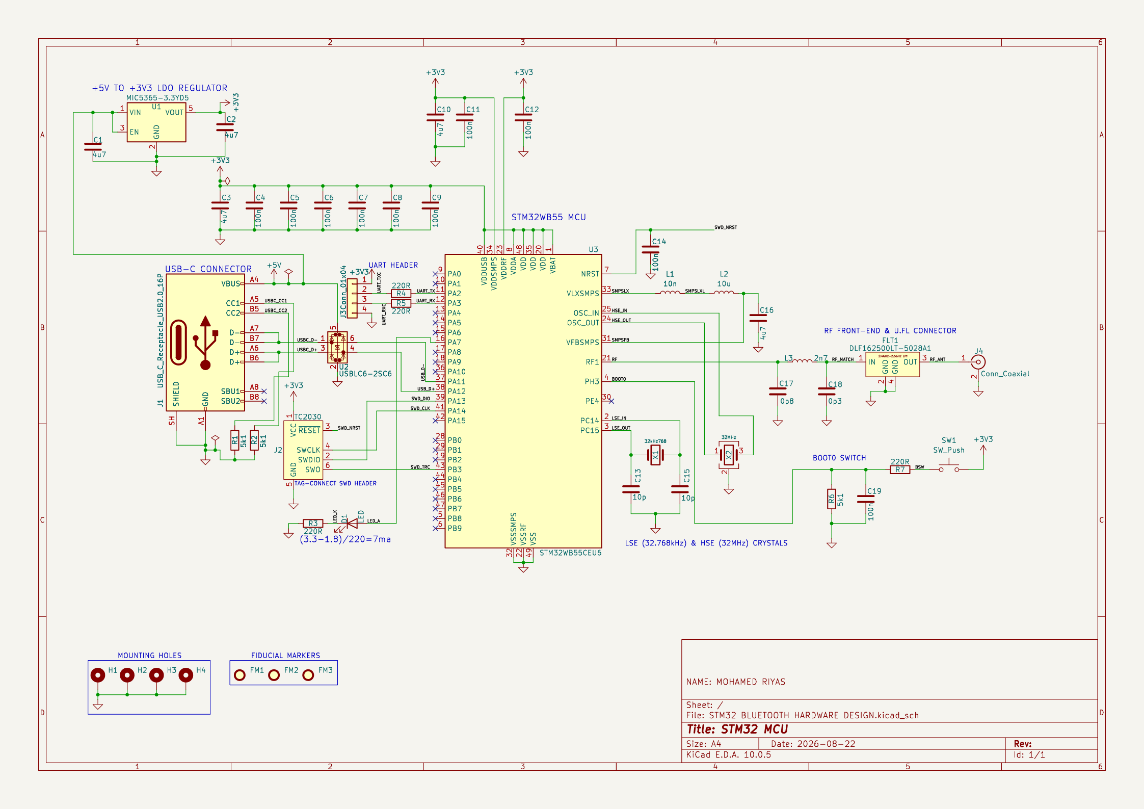
STM32WB55 uses an internal buck converter. VLXSMPS pin drives the inductor, SMPSFB senses feedback, and VFBSMPS stabilizes output.This lowers current draw and heat, especially important for battery‑powered designs.
Working:
MCU generates Bluetooth RF signal → passes through matching network → filtered → sent to antenna. Impedance control (50 Ω single‑ended) ensures maximum power transfer and minimal reflection.
The schematic illustrates the complete STM32WB55CEU6 Bluetooth hardware design, including power supply (LDO + SMPS), USB‑C interface with ESD protection, SWD debug header, RF front‑end with matching network and U.FL antenna connector, and peripheral components (UART, LED, crystals, push button).
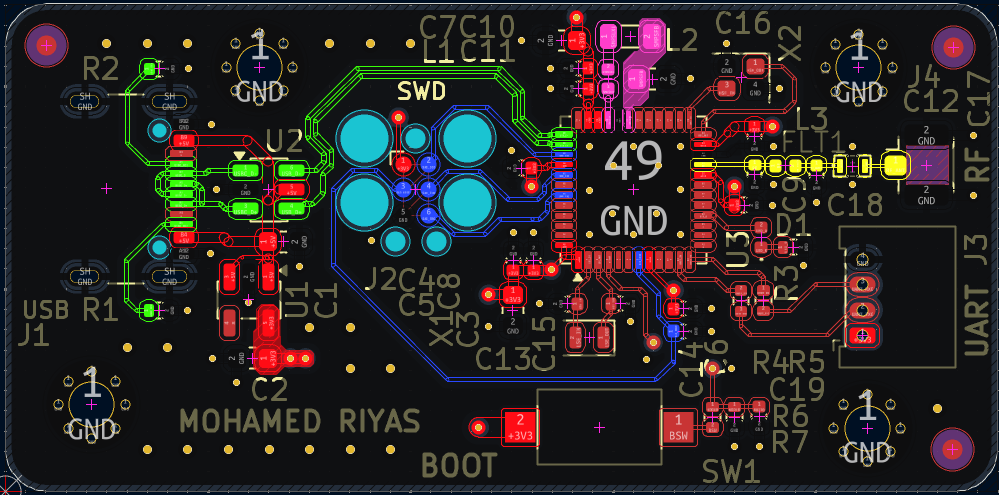
The top layer layout shows the placement of STM32WB55CEU6, USB‑C connector, RF front‑end, SWD header, and supporting components.
Silkscreen markings highlight pin labels and orientation for assembly.
Copper pour on this layer is dedicated to the GND plane, ensuring stable return paths and reduced EMI.
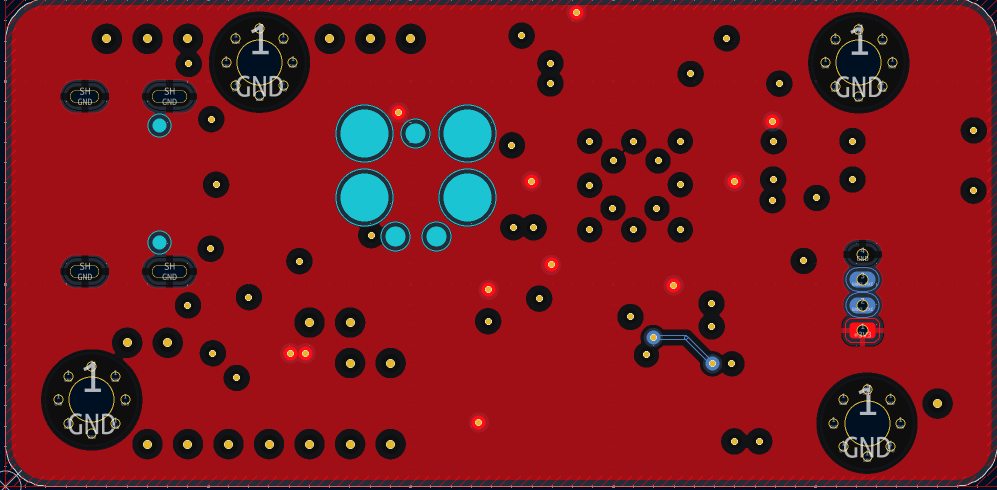
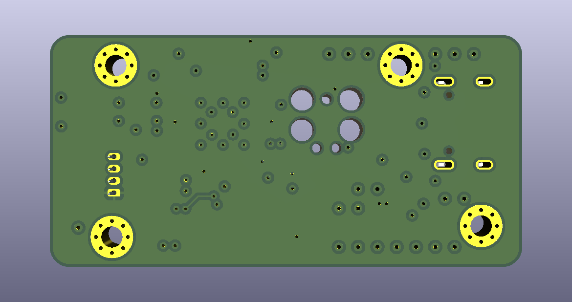
The bottom layer layout highlights the routing of power planes and supporting traces.
This layer is dedicated to the power plane, ensuring stable distribution of 3.3V and other supply rails across the board.
It complements the three GND planes (Front, In1, In2) by providing a clean separation of power and ground, improving signal integrity and reducing noise.
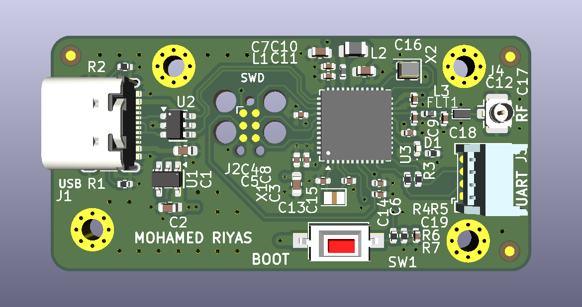
The 3D views provide a realistic visualization of the PCB assembly.
They include custom STEP models for the STM32WB55CEU6 microcontroller, the DLF162500LT‑5028A1 RF filter, and the 32.768 kHz crystal.
These models ensure accurate mechanical alignment, proper component clearance, and a professional preview of the final board.
| Qty | Value | Footprint | References |
|---|---|---|---|
| 10 | 100n | Capacitor_SMD:C_0402_1005Metric | C4, C5, C6, C7, C8, C9, C11, C12, C14, C19 |
| 5 | 4u7 | Capacitor_SMD:C_0603_1608Metric | C1, C2, C3, C10, C16 |
| 4 | 220R | Resistor_SMD:R_0402_1005Metric | R3, R4, R5, R7 |
| 4 | MountingHole_Pad | MountingHole:MountingHole_2.2mm_M2_Pad_Via | H1, H2, H3, H4 |
| 3 | 5k1 | Resistor_SMD:R_0402_1005Metric | R1, R2, R6 |
| 3 | Fiducial | Fiducial:Fiducial_1mm_Mask2mm | FM1, FM2, FM3 |
| 2 | 10p | Capacitor_SMD:C_0402_1005Metric | C13, C15 |
| 1 | 0p3 | Capacitor_SMD:C_0402_1005Metric | C18 |
| 1 | 0p8 | Capacitor_SMD:C_0402_1005Metric | C17 |
| 1 | 10n | Inductor_SMD:L_0402_1005Metric | L1 |
| 1 | 10u | Inductor_SMD:L_0805_2012Metric | L2 |
| 1 | 2n7 | Inductor_SMD:L_0402_1005Metric | L3 |
| 1 | 32MHz | Crystal:Crystal_SMD_2016-4Pin_2.0x1.6mm | X2 |
| 1 | 32kHz768 | Crystal:Crystal_SMD_2012-2Pin_2.0x1.2mm | X1 |
| 1 | Conn_01x04 | Connector_Molex:Molex_PicoBlade_53048-0410_1x04_P1.25mm_Horizontal | J3 |
| 1 | Conn_Coaxial | Connector_Coaxial:U.FL_Hirose_U.FL-R-SMT-1_Vertical | J4 |
| 1 | DLF162500LT-5028A1 | STM32 BLUETOOTH HARDWARE DESIGN_PCBFootprints:DLF162500LT-5028A1 | FLT1 |
| 1 | LED | LED_SMD:LED_0402_1005Metric | D1 |
| 1 | MIC5365-3.3YD5 | Package_TO_SOT_SMD:TSOT-23-5 | U1 |
| 1 | STM32WB55CEU6 | Package_DFN_QFN:QFN-48-1EP_7x7mm_P0.5mm_EP5.6x5.6mm | U3 |
| 1 | SW_Push | Button_Switch_SMD:SW_SPST_CK_RS282G05A3 | SW1 |
| 1 | TC2030 | Connector:Tag-Connect_TC2030-IDC-FP_2x03_P1.27mm_Vertical | J2 |
| 1 | USBLC6-2SC6 | Package_TO_SOT_SMD:SOT-23-6 | U2 |
| 1 | USB_C_Receptacle_USB2.0_16P | Connector_USB:USB_C_Receptacle_GCT_USB4105-xx-A_16P_TopMnt_Horizontal | J1 |


OdaiJ/stm32-bt-board
My attempt at following the Phil's Lab KiCad V7 tutorial on YouTube

shivamtiwari020505/stm32wb55-ble-dev-board
Custom STM32WB55 development board integrating 2.4GHz BLE 5.x, LPUART, I2C, and UART via RS232/DB9 for PC and industrial machine interfacing. Designed to bridge modern wireless IoT with legacy wired systems.


justinfederico/STM32testPCB
Custom STM32WB microcontroller to practice my PCB schematic and layout skills. Looking to get it printed soon! Bear in mind that this is an ameuter project, so there will probably be errors aplenty.
It measures 49 × 24 mm and has 4 copper layers, 1.58 mm thick.
48 parts, built around the STM32WB55CEU6, DLF162500LT-5028A1, MIC5365-3.3YD5-TR and USBLC6-2SC6. The full list of its parts is on this page, with links to each part's symbol and footprint where PCBKit's library has them.
From the riyassadiq11/STM32_Bluetooth_Hardware_Design_PCB repository on GitHub, at the commit this page was made from: the board is STM32 BLUETOOTH HARDWARE DESIGN/STM32 BLUETOOTH HARDWARE DESIGN.kicad_pcb and its schematic STM32 BLUETOOTH HARDWARE DESIGN/STM32 BLUETOOTH HARDWARE DESIGN.kicad_sch. PCBKit opens the board in the browser, with nothing to install.
Its repository publishes it under the MIT licence: you may reuse it on that licence's terms (keep the author's notice, and for a copyleft licence share your changes alike).