
4 layers68.6 × 94 mm
Nucleo144AudioBreakout
rhinocerose/breakout-boards
Some small adapter boards to help with prototyping SMT packages on a breadboard.
59 parts1

 rhinocerose/breakout-boards1
Some small adapter boards to help with prototyping SMT packages on a breadboard.
Encoder debouncing is an open-source printed circuit board by rhinocerose, from the rhinocerose/breakout-boards repository on GitHub. It is a 2-layer board of 25.4 × 25.4 mm with 18 parts on 14 nets, routed with 118 tracks and 14 vias.
It is built around the 74HC14 and M2.5. Its parts include 6 resistors, 4 capacitors, 2 connectors, 1 IC and 1 switch.
Some small adapter boards to help with prototyping SMT packages on a breadboard.
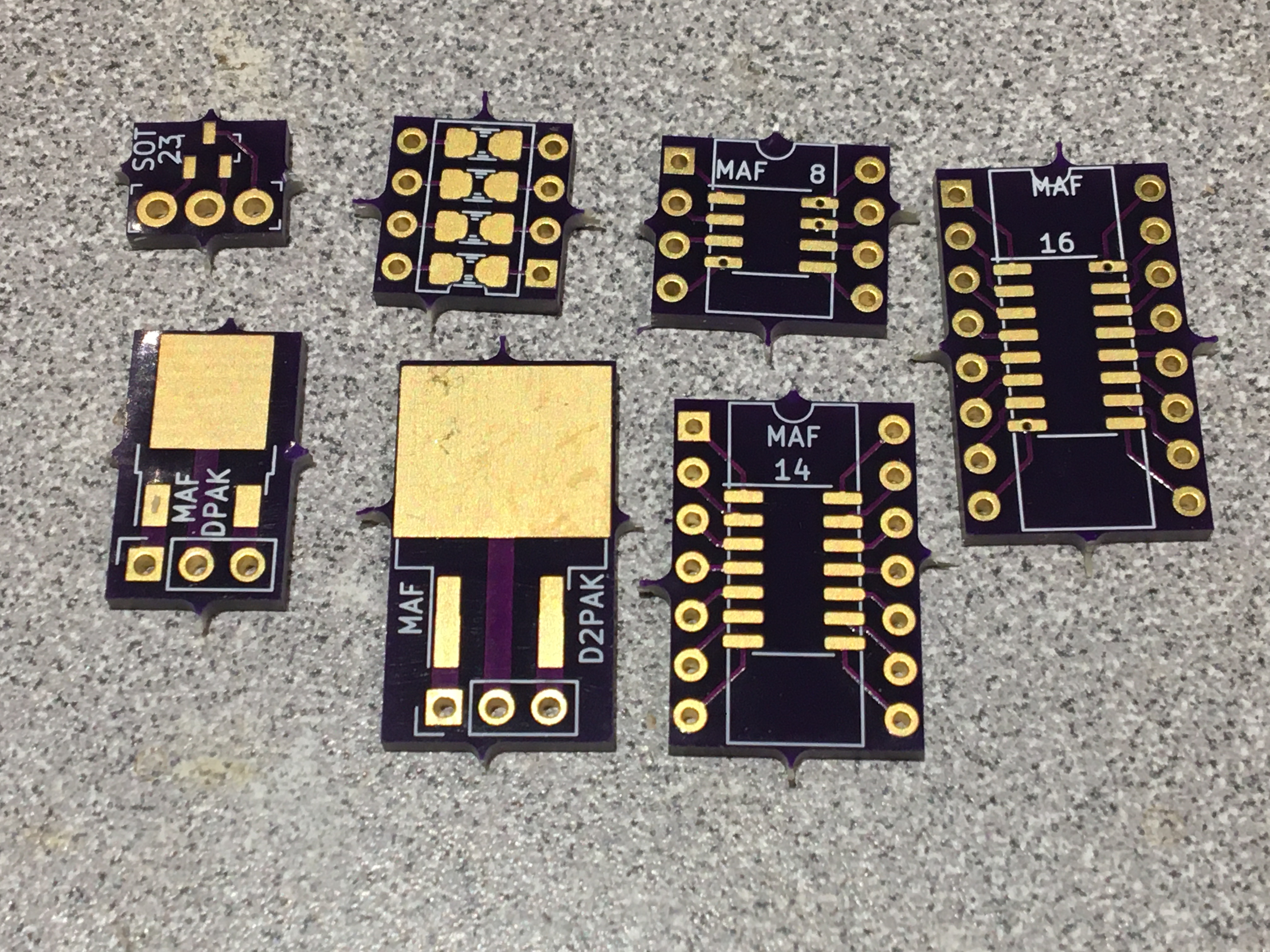
I used KiCad to draw these.
Usually you would start with a schematic and a symbol and then lay out the PCB.
In this case I just opened the PCBNew application and ad-hoc added the footprints and then drew traces to wire them up.
I will add more footprints as I need them.
I Used OSHPark to have these made. Mostly because I don't have a setup to make my own boards.
For convenience, I shared the uploaded board projects:
| Part | Link |
|---|---|
| SOIC-8 | https://oshpark.com/shared_projects/7HKL5QIy |
| SOIC-14 | https://oshpark.com/shared_projects/QcCbjX4y |
| SOIC-16 | https://oshpark.com/shared_projects/uA6pM7Gf |
| SOT-23 | https://oshpark.com/shared_projects/ge0wqWtr |
| SOT23-5 | https://oshpark.com/shared_projects/e4J13SY4 |
| SMD-6 | https://oshpark.com/shared_projects/h2nZ3u9U |
| TO-252 (DPAK) | https://oshpark.com/shared_projects/cjtZqxyG |
| TO-263 (D2PAK) | https://oshpark.com/shared_projects/tPH46DG8 |
| 0406/0603/0806/1204 x4 | https://oshpark.com/shared_projects/MdGxr2ob |
| 0406/0603/0806/1204 x7 | https://oshpark.com/shared_projects/SLZF8xvz |
I am not affiliated by or sponsored by OSHPark. I just am really happy with the kind of service they provide.
These steps assume you have
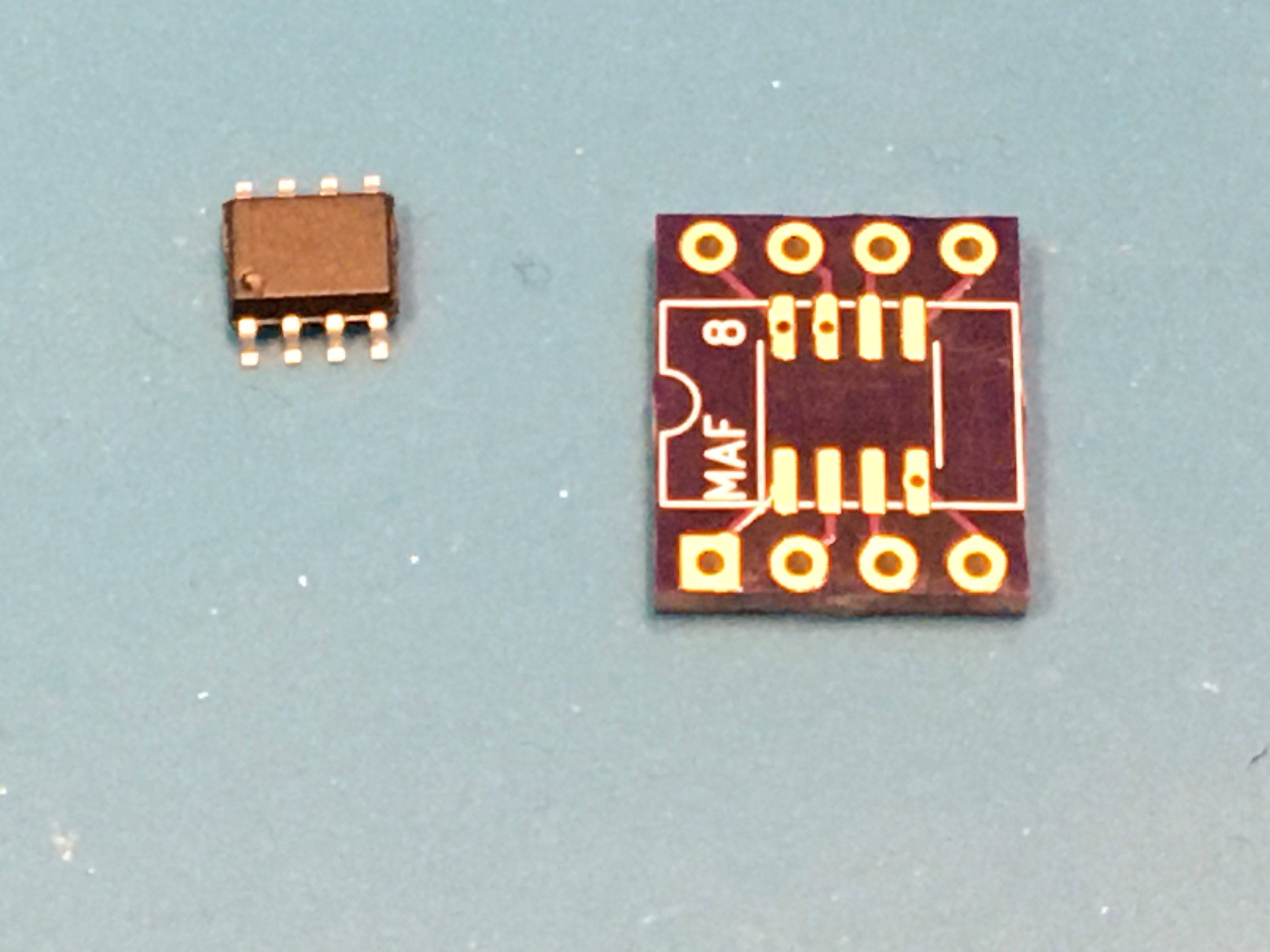
Start by soldering the SMT device to the PCB
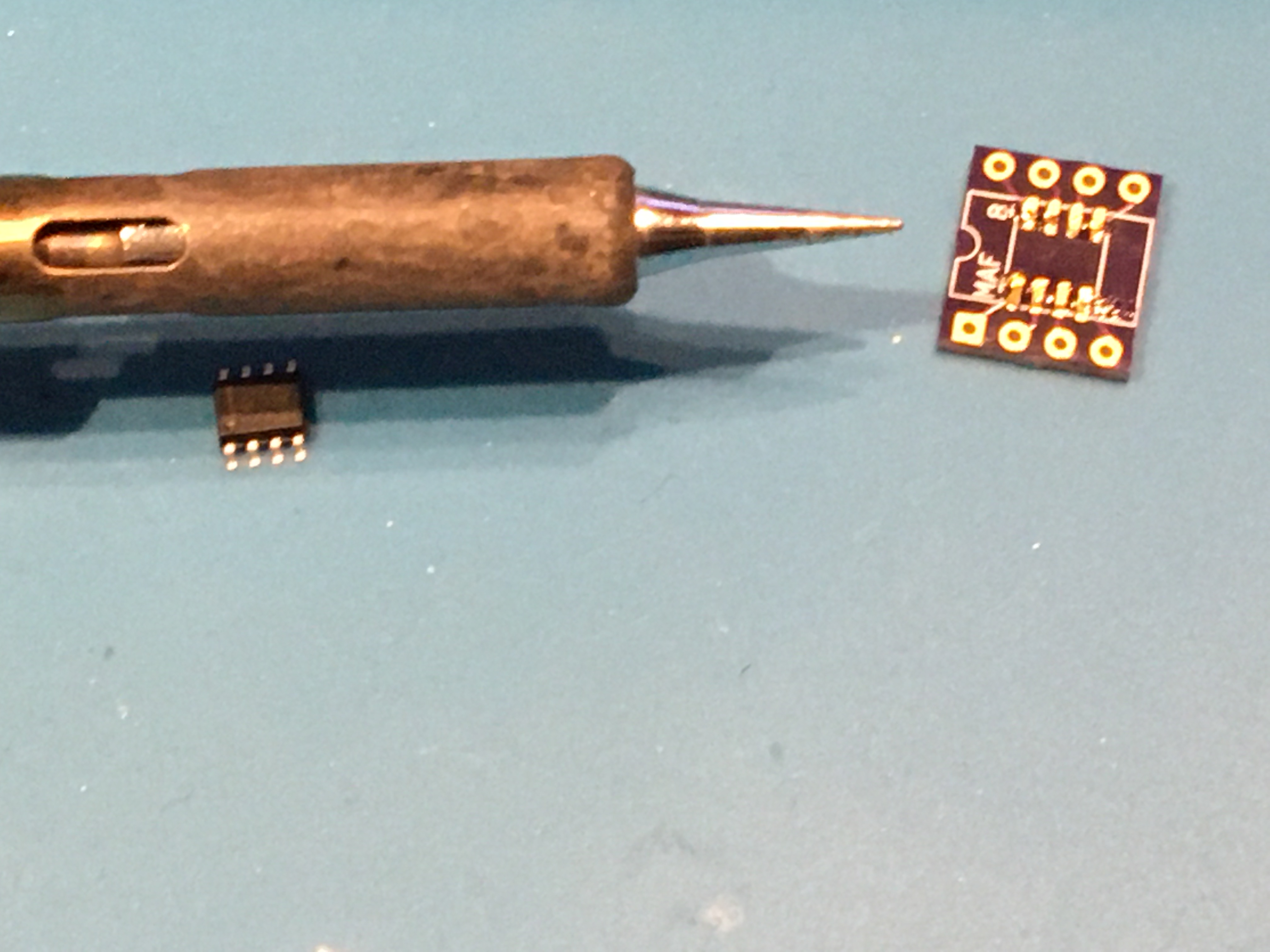
I have a hot air solder station. I use a fine point solder iron here, as this is more likely what most people would have.
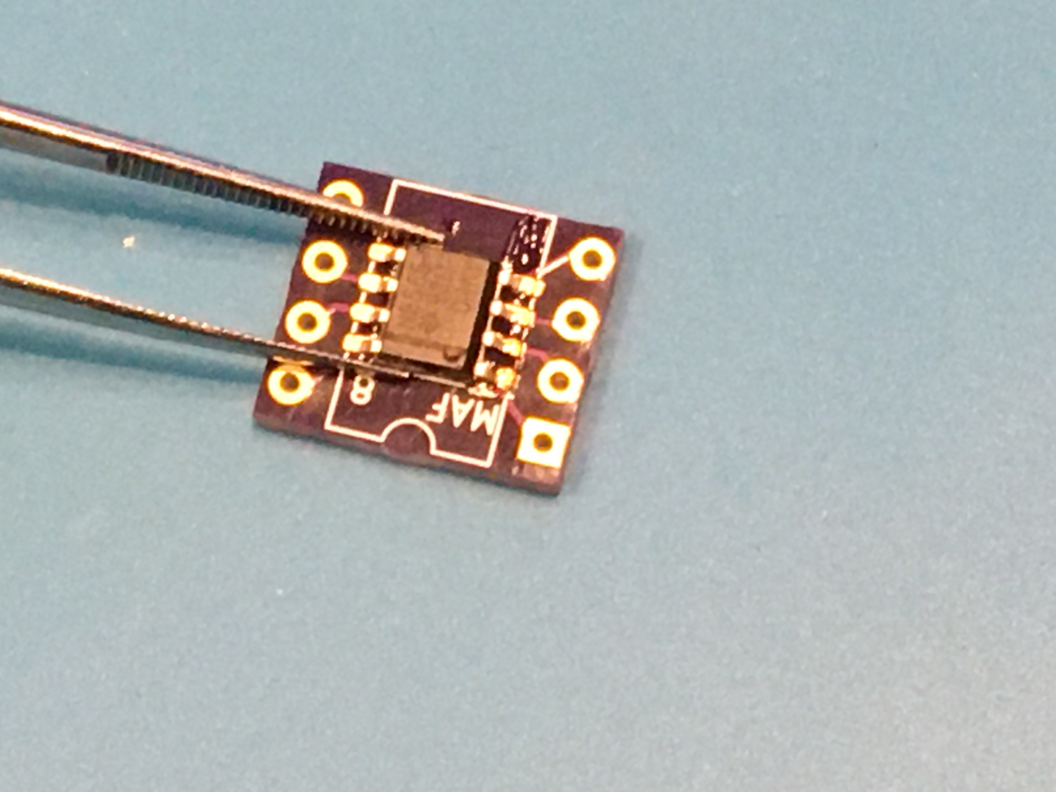
I like to use a pair of tweezers
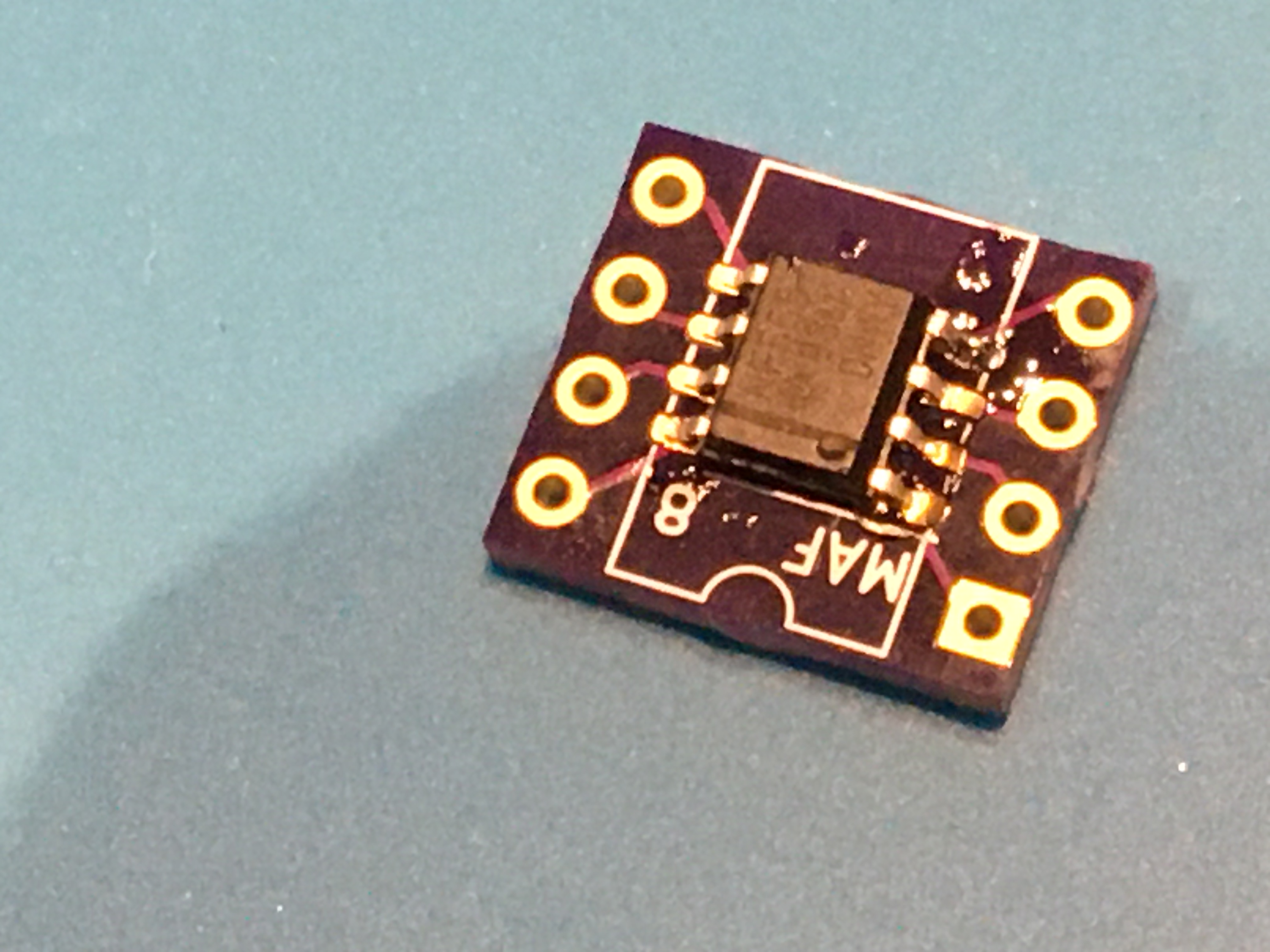
This is the hard part and takes practise.
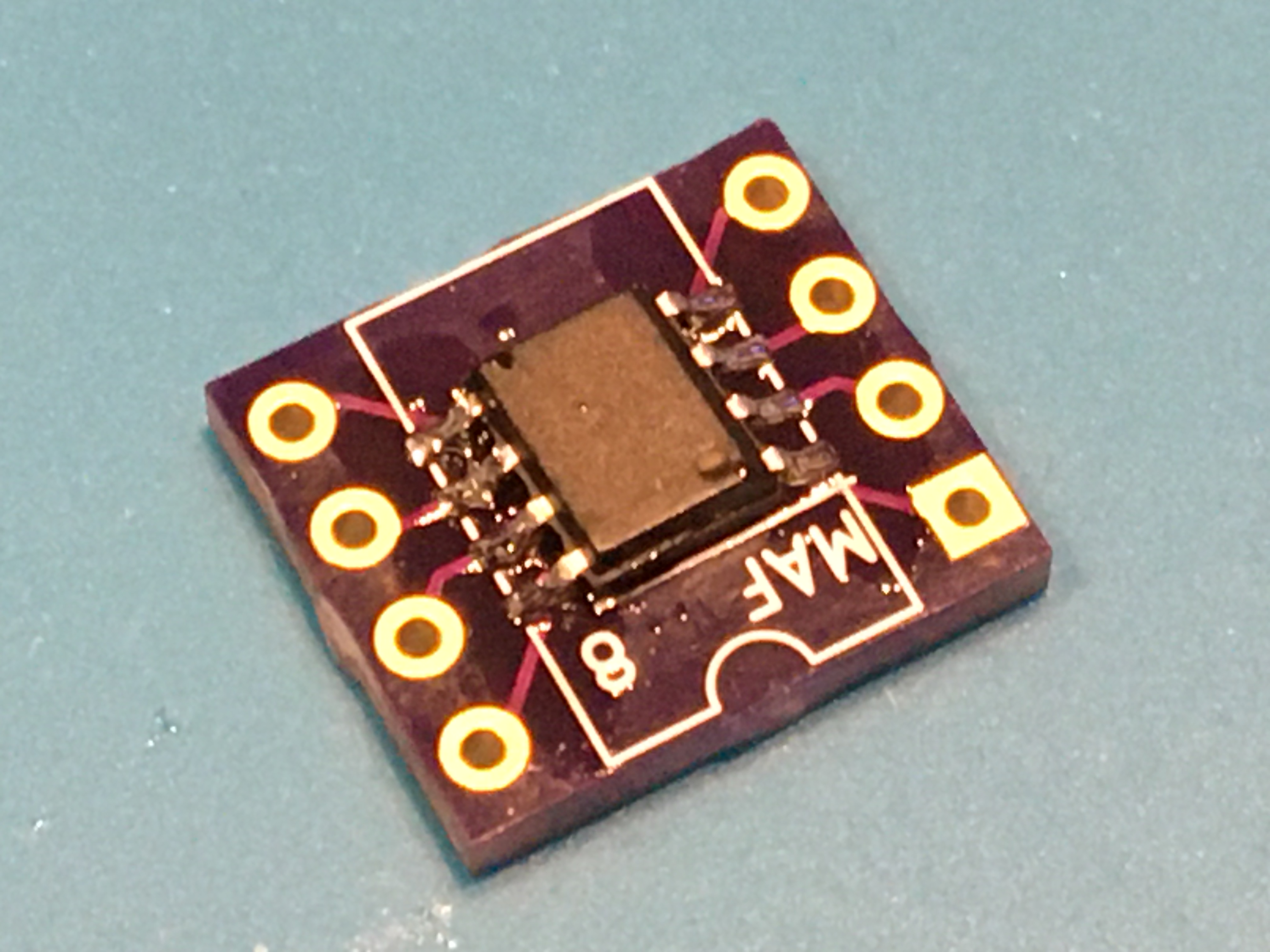
This part is fun. The solder mask prevents the solder from sticking between the pads. The flux helps the solder to flow evenly over each pin. We want to use as little solder as possible here.
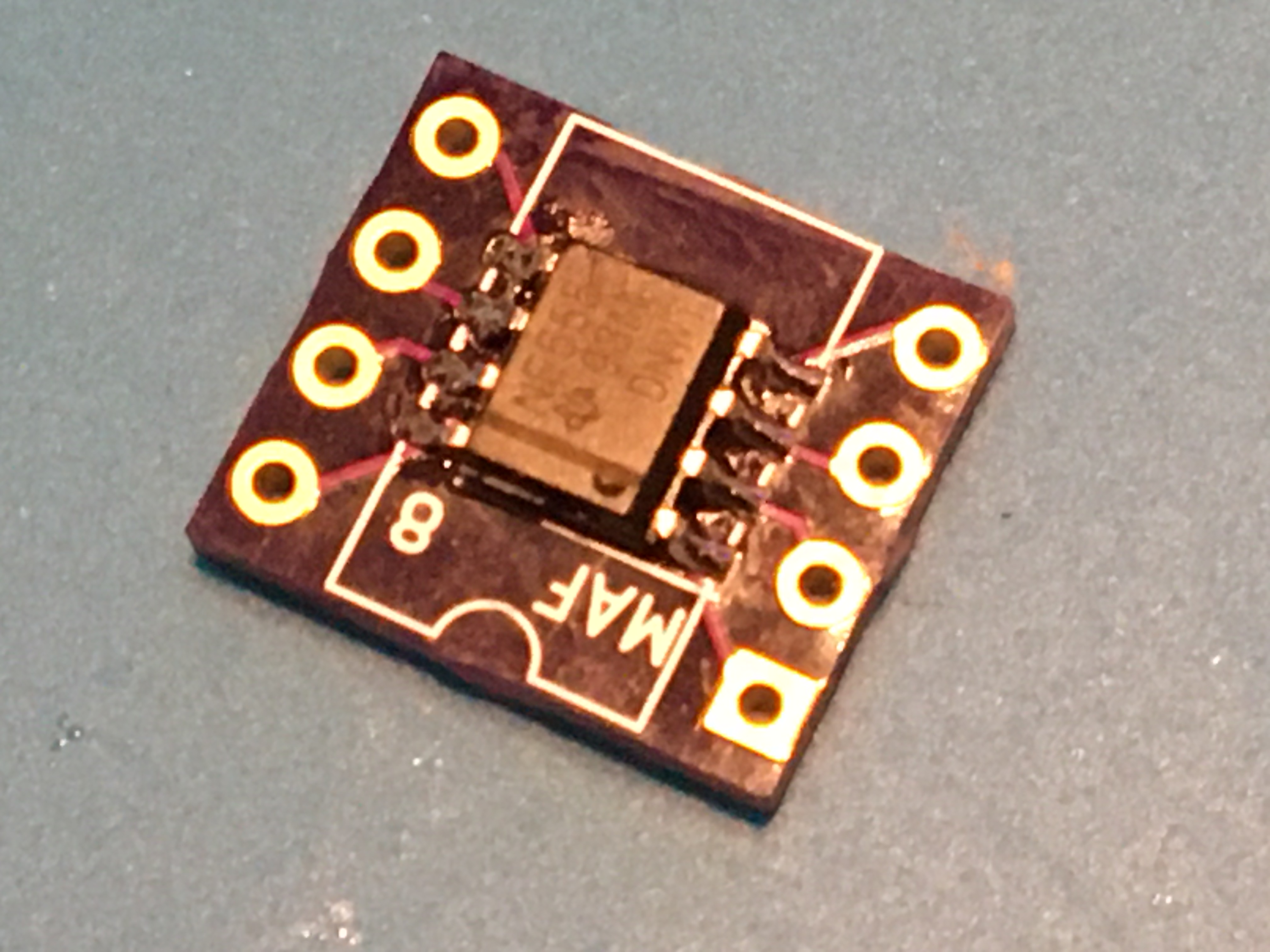
If your device is static sensitive, work on a grounded or ESD safe surface.
(Optional) : Where applicable, if you would like a decoupling capacitor, solder the 0603 package capacitor to the back
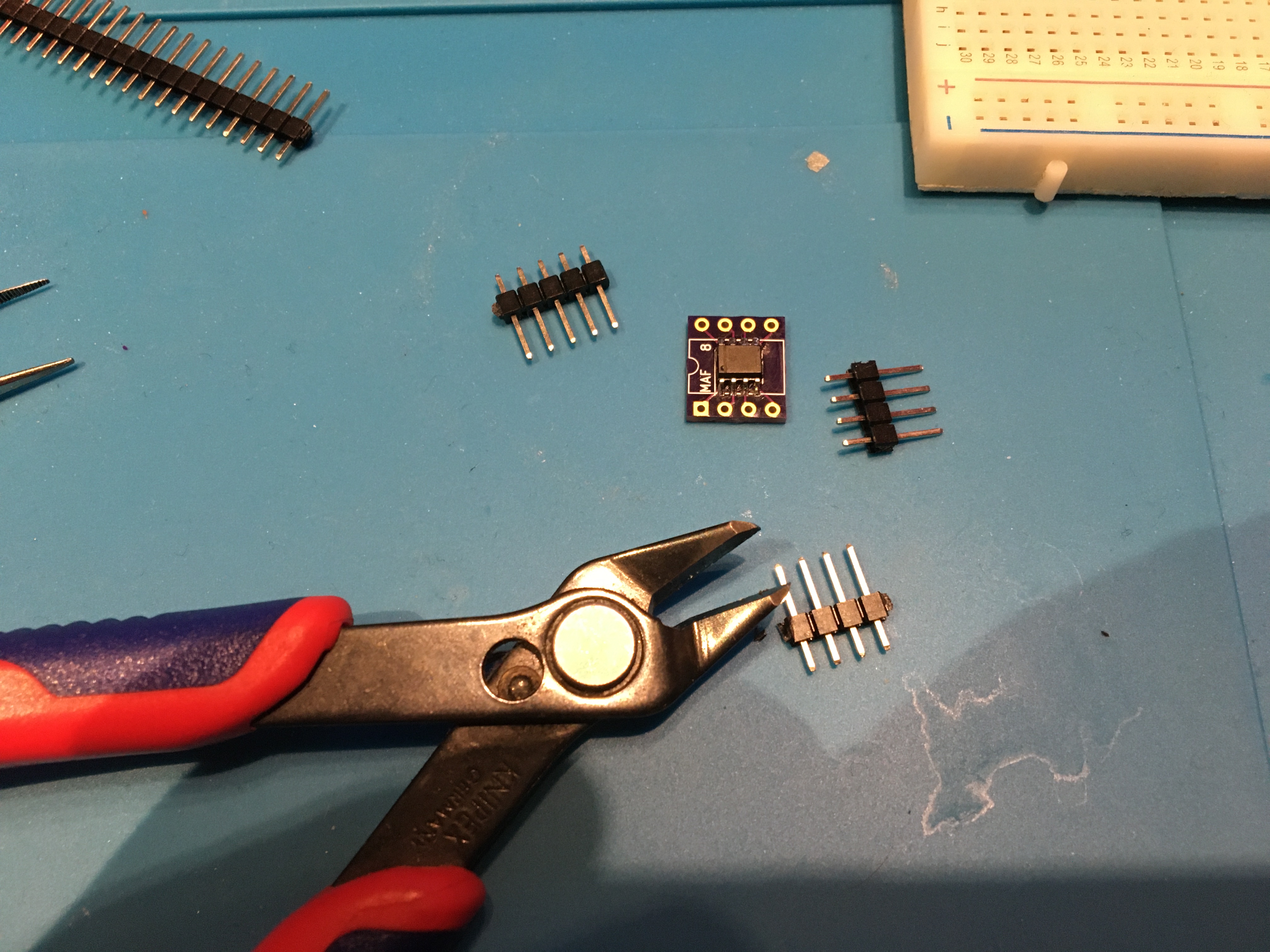
Cut stock pin headers as needed.
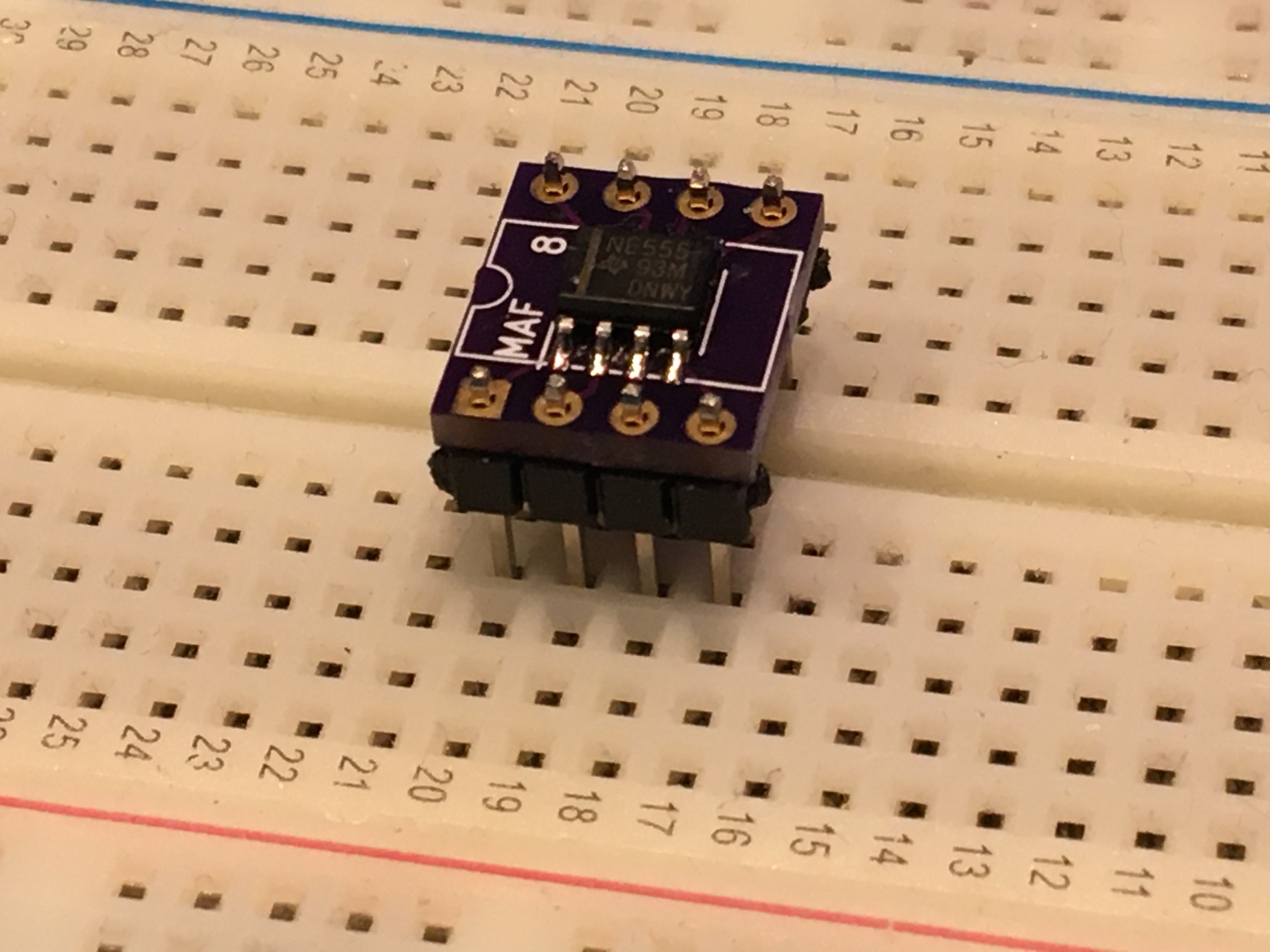
But do not solder with a lot of heat on the breadboard, it migh melt the breadboard socket guides.
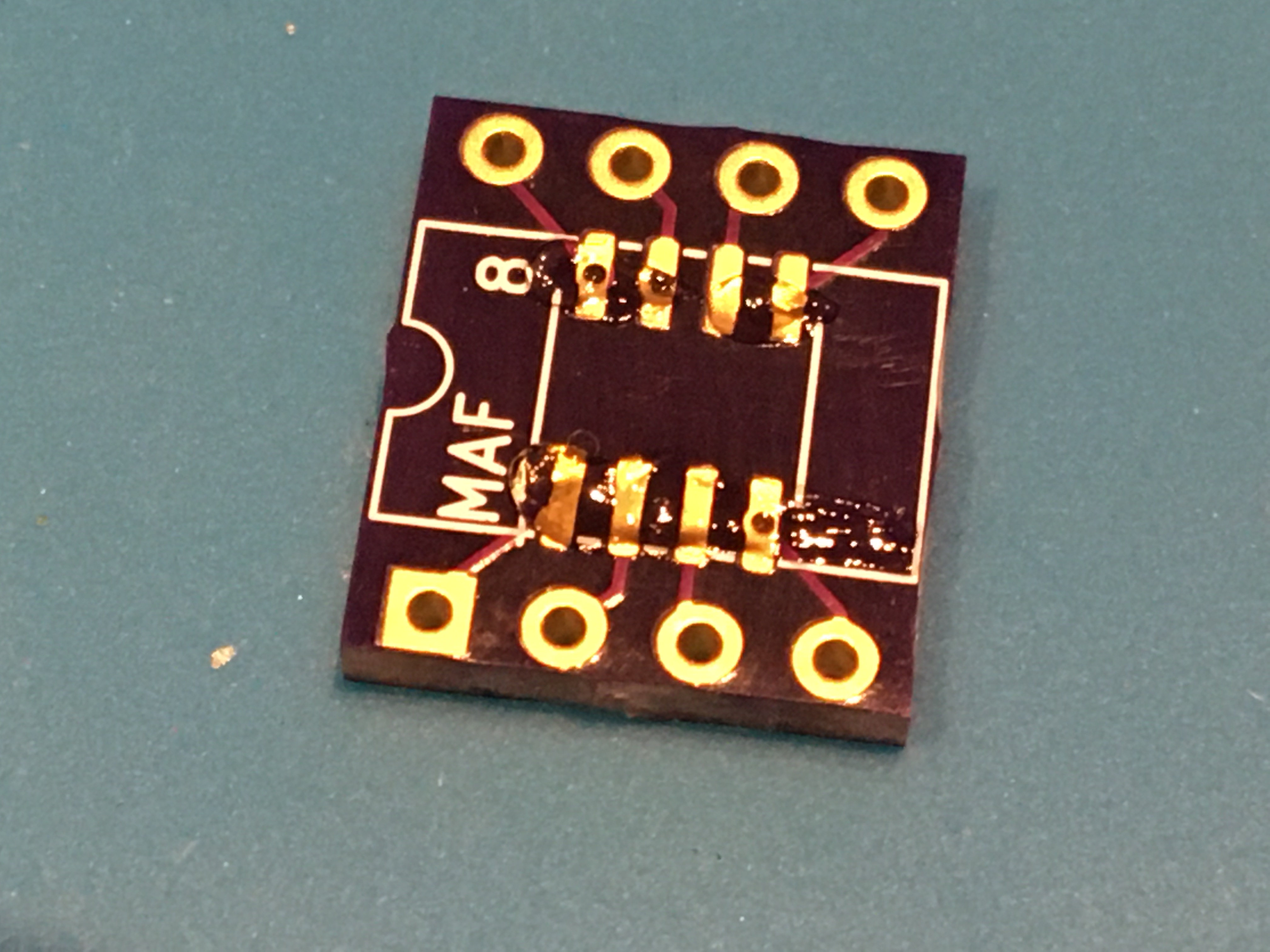
And then the final result:
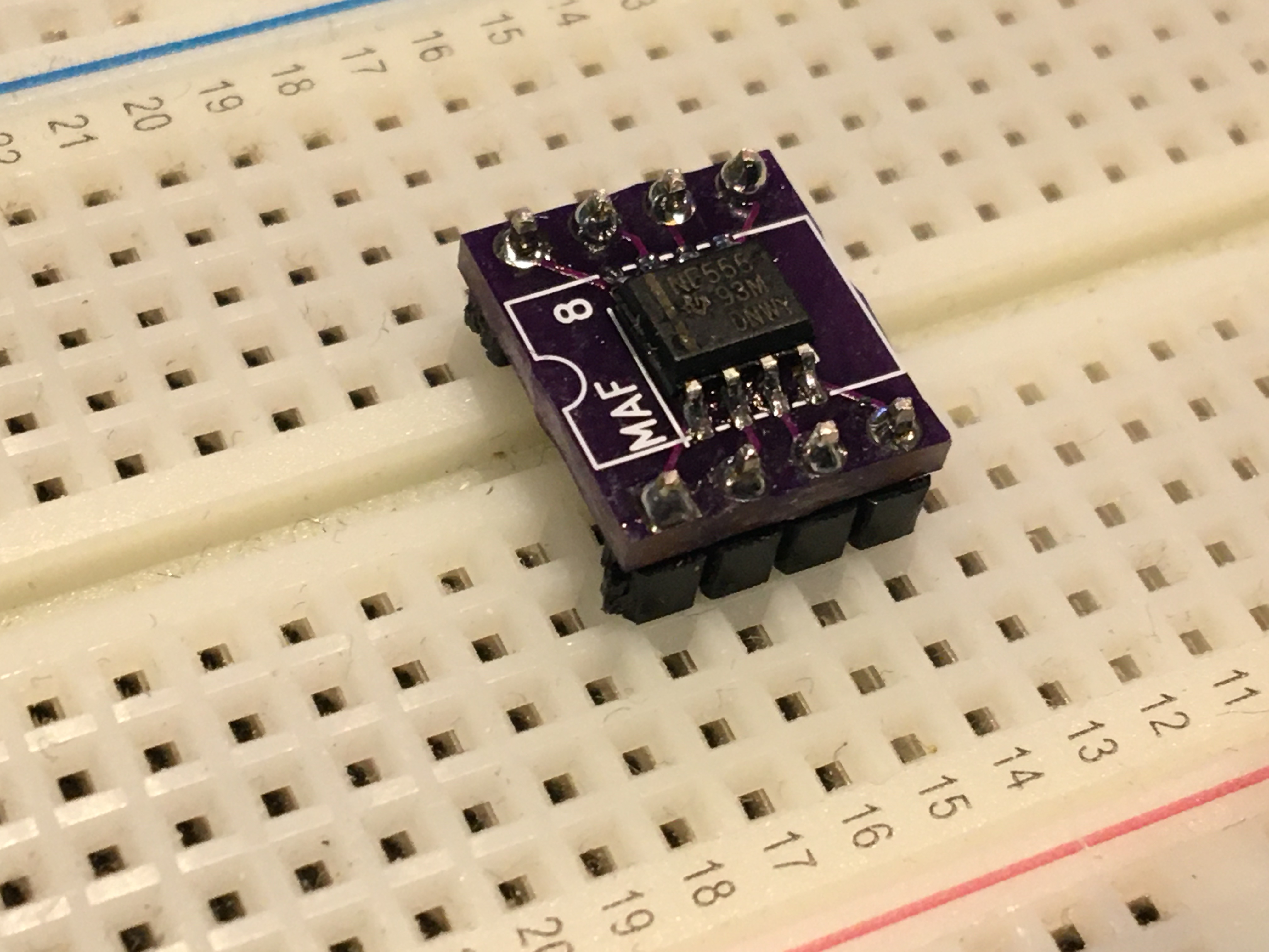
It is the similar idea for the other packages, just with more or different pins really.
| Qty | Value | Footprint | References |
|---|---|---|---|
| 6 | 10K | Resistor_SMD:R_0603_1608Metric_Pad0.98x0.95mm_HandSolder | R1, R2, R3, R4, R5, R6 |
| 4 | 100nF | Capacitor_SMD:C_0603_1608Metric_Pad1.08x0.95mm_HandSolder | C1, C2, C3, C4 |
| 4 | M2.5 | MountingHole:MountingHole_2.7mm_M2.5_ISO7380_Pad_TopBottom | H1, H2, H3, H4 |
| 2 | Header | Connector_PinHeader_2.54mm:PinHeader_1x05_P2.54mm_Vertical | J1, J2 |
| 1 | 74HC14 | Package_SO:SOIC-14_3.9x8.7mm_P1.27mm | U1 |
| 1 | EC11 | Rotary_Encoder:RotaryEncoder_Alps_EC11E-Switch_Vertical_H20mm | SW1 |
rhinocerose/breakout-boards
Some small adapter boards to help with prototyping SMT packages on a breadboard.

rhinocerose/breakout-boards
Some small adapter boards to help with prototyping SMT packages on a breadboard.

rhinocerose/breakout-boards
Some small adapter boards to help with prototyping SMT packages on a breadboard.

rhinocerose/breakout-boards
Some small adapter boards to help with prototyping SMT packages on a breadboard.

rhinocerose/breakout-boards
Some small adapter boards to help with prototyping SMT packages on a breadboard.

rhinocerose/breakout-boards
Some small adapter boards to help with prototyping SMT packages on a breadboard.

rhinocerose/breakout-boards
Some small adapter boards to help with prototyping SMT packages on a breadboard.

rhinocerose/breakout-boards
Some small adapter boards to help with prototyping SMT packages on a breadboard.

rhinocerose/breakout-boards
Some small adapter boards to help with prototyping SMT packages on a breadboard.

rhinocerose/breakout-boards
Some small adapter boards to help with prototyping SMT packages on a breadboard.

rhinocerose/breakout-boards
Some small adapter boards to help with prototyping SMT packages on a breadboard.

rhinocerose/breakout-boards
Some small adapter boards to help with prototyping SMT packages on a breadboard.

sbstnh/programmable_precision_resistor
A SCPI programmable precision resistor


Spirit532/studio_mic
A simple, easy to build preamplifier for any true condenser capsule, to make a condenser microphone


gmcn42/clumsyMIDI
A THT-only Raspberry Pi expansion board containing a MIDI interface, DAC, and OLED display

DvidMakesThings/HW_PDNode-600-Pro
The PDNode-600 is a professional-grade, 600W USB Power Delivery Unit designed specifically for compact 10-inch rack systems, targeting embedded developers, homelab enthusiasts, test benches, and smart infrastructure.


It measures 25.4 × 25.4 mm and has 2 copper layers, 1.6 mm thick.
18 parts, built around the 74HC14 and M2.5. The full list of its parts is on this page, with links to each part's symbol and footprint where PCBKit's library has them.
From the rhinocerose/breakout-boards repository on GitHub, at the commit this page was made from: the board is input-output/Schmitt-Encoder-Debouncing-Module/project_files/0603/encoder_debouncing.kicad_pcb. PCBKit opens the board in the browser, with nothing to install.
Its repository states no licence, so its author keeps all rights: ask rhinocerose before reusing the design.