2 layers91.5 × 100 mm
Lights pcb
QuinnFreedman/modular
A collection of free & open source DIY synthesizer module designs for Eurorack
59 parts116

 qu1j0t3/vector_gen13
In first version of PCB there is a bug that leaves U6 Vss/Vdd pins floating and U5 Vdd floating:
Vector gen is an open-source printed circuit board by qu1j0t3, from the qu1j0t3/vector_gen repository on GitHub. It is a 2-layer board of 91.4 × 101.6 mm with 103 parts on 101 nets, routed with 779 tracks and 6 vias.
It is built around the MCP4922-E/P, MCP6292-E/P and TL072IP, with the 74HC86D, LM336 and MAX4544CPA+ among its other parts. Its parts include 31 resistors, 22 capacitors, 13 ICs, 12 connectors and 1 diode.


In first version of PCB there is a bug that leaves U6 Vss/Vdd pins floating and U5 Vdd floating:
Due to redrilling of X and Z BNC footprints:
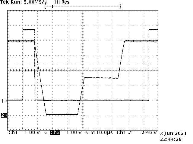
main.c)display_list.h, defines DAC_COEFF_X_ADJ and DAC_COEFF_Y_ADJRun test program 4
Connect DVM ground to ground point (see test 1b)
Connect DVM + lead to XINTEG test point, measure voltage, e.g. 2.4894 (XI)
Move DVM + lead to YINTEG test point, measure voltage, e.g. 2.4900 (YI)
Move DVM + lead to XLIMIT test point, measure voltage, e.g. 2.4955 (XL)
Move DVM + lead to YLIMIT test point, measure voltage, e.g. 2.5054 (YL)
Noting that Limit DACS use gain x2 i.e. 1 unit = 5/4096 V
Compute limit adjustment for X = 4096*(XI - XL)/5 = -5
adjustment for Y = 4096*(YI - YL)/5 = -13
Set these values in display_list.h, defines DAC_LIMIT_X_ADJ and DAC_LIMIT_Y_ADJ
Run test program 4b
Check that XLIMIT and YLIMIT are within about 2 mV of XINTEG and YINTEG
| Qty | Value | Footprint | References |
|---|---|---|---|
| 14 | 1u | Capacitor_THT:C_Disc_D5.0mm_W2.5mm_P2.50mm | C1, C2, C3, C4, C5, C7, C9, C10, C15, C16, C19, C20, C21, C22 |
| 14 | TestPoint | TestPoint:TestPoint_THTPad_2.5x2.5mm_Drill1.2mm | PB0, PC4, PC5, STOP1, VREF2.5, X1, XCOEFF1, XINTEG1, XLIMIT1, Y1, YCOEFF1, YINTEG1, YLIMIT1, Z1 |
| 8 | 33k | Resistor_THT:R_Axial_DIN0207_L6.3mm_D2.5mm_P10.16mm_Horizontal | R8, R9, R10, R11, R17, R18, R19, R20 |
| 7 | 10k | Resistor_THT:R_Axial_DIN0207_L6.3mm_D2.5mm_P10.16mm_Horizontal | R4, R6, R16, R28, R29, R30, R33 |
| 6 | 15k | Resistor_THT:R_Axial_DIN0207_L6.3mm_D2.5mm_P10.16mm_Horizontal | R5, R7, R22, R23, R24, R25 |
| 4 | .1u | Capacitor_THT:C_Disc_D5.0mm_W2.5mm_P2.50mm | C13, C14, C17, C18 |
| 4 | MountingHole | MountingHole:MountingHole_3.2mm_M3 | H1, H2, H3, H4 |
| 3 | 2.2k | Resistor_THT:R_Axial_DIN0207_L6.3mm_D2.5mm_P10.16mm_Horizontal | R1, R26, R27 |
| 3 | Conn_Coaxial | Connector_Coaxial:BNC_TEConnectivity_1478204_Vertical | XOUT1, YOUT1, ZOUT1 |
| 3 | MCP4922 | Package_DIP:DIP-14_W7.62mm_Socket | U1, U10, U11 |
| 2 | 100k? to be determined | Resistor_THT:R_Axial_DIN0207_L6.3mm_D2.5mm_P10.16mm_Horizontal | R12, R13 |
| 2 | 100u | Capacitor_THT:CP_Radial_D6.3mm_P2.50mm | C6, C8 |
| 2 | 10n | Capacitor_THT:C_Rect_L7.0mm_W2.5mm_P5.00mm | C11, C12 |
| 2 | 47 | Resistor_THT:R_Axial_DIN0207_L6.3mm_D2.5mm_P10.16mm_Horizontal | R34, R35 |
| 2 | 74LS07 | Package_DIP:DIP-14_W7.62mm_Socket | U16, U17 |
| 1 | 10k | Potentiometer_THT:Potentiometer_TT_P0915N | RV1 |
| 1 | 22k | Resistor_THT:R_Axial_DIN0207_L6.3mm_D2.5mm_P10.16mm_Horizontal | R21 |
| 1 | 2N3904 | Package_TO_SOT_THT:TO-92_Inline_Wide | Q1 |
| 1 | 330 | Resistor_THT:R_Axial_DIN0207_L6.3mm_D2.5mm_P10.16mm_Horizontal | R2 |
| 1 | 4.7k | Resistor_THT:R_Axial_DIN0207_L6.3mm_D2.5mm_P10.16mm_Horizontal | R3 |
| 1 | 4019 | Package_DIP:DIP-16_W7.62mm_Socket | U12 |
| 1 | 4066 | Package_DIP:DIP-14_W7.62mm_Socket | U5 |
| 1 | 74HC86 | Package_DIP:DIP-14_W7.62mm_Socket | U14 |
| 1 | ARDUINO J1 | Connector_PinHeader_2.54mm:PinHeader_1x08_P2.54mm_Vertical | J10 |
| 1 | ARDUINO J1 3.3V | Connector_PinHeader_2.54mm:PinHeader_1x08_P2.54mm_Vertical | J5 |
| 1 | ARDUINO J2 | Connector_PinHeader_2.54mm:PinHeader_1x06_P2.54mm_Vertical | J9 |
| 1 | ARDUINO J2 3.3V | Connector_PinHeader_2.54mm:PinHeader_1x06_P2.54mm_Vertical | J3 |
| 1 | ARDUINO J3 | Connector_PinHeader_2.54mm:PinHeader_1x08_P2.54mm_Vertical | J8 |
| 1 | ARDUINO J3 3.3V | Connector_PinHeader_2.54mm:PinHeader_1x08_P2.54mm_Vertical | J2 |
| 1 | ARDUINO POWER | Connector_PinHeader_2.54mm:PinHeader_1x06_P2.54mm_Vertical | J7 |
| 1 | ARDUINO POWER 3.3V | Connector_PinHeader_2.54mm:PinHeader_1x06_P2.54mm_Vertical | J1 |
| 1 | Conn_01x02 | Connector_PinSocket_2.54mm:PinSocket_1x02_P2.54mm_Vertical | J12 |
| 1 | Conn_01x02_Female | Connector_PinHeader_2.54mm:PinHeader_1x02_P2.54mm_Vertical | J4 |
| 1 | Conn_01x03 | Connector_Molex:Molex_KK-396_A-41791-0003_1x03_P3.96mm_Vertical | J6 |
| 1 | Conn_01x08 | Connector_PinHeader_2.54mm:PinHeader_1x08_P2.54mm_Vertical | J11 |
| 1 | LED | LED_THT:LED_D3.0mm | D1 |
| 1 | LM319 | Package_DIP:DIP-14_W7.62mm_Socket | U9 |
| 1 | LM336 | Package_TO_SOT_THT:TO-92_HandSolder | U13 |
| 1 | MAX4544 | Package_DIP:DIP-8_W7.62mm_Socket | U19 |
| 1 | MCP6292 | Package_DIP:DIP-8_W7.62mm_Socket | U6 |
| 1 | R_Network09_US | Resistor_THT:R_Array_SIP10 | RN2 |
| 1 | TL072IP | Package_DIP:DIP-8_W7.62mm_Socket | U8 |
It measures 91.4 × 101.6 mm and has 2 copper layers, 1.6 mm thick.
103 parts, built around the MCP4922-E/P, MCP6292-E/P, TL072IP and 74HC86D. The full list of its parts is on this page, with links to each part's symbol and footprint where PCBKit's library has them.
From the qu1j0t3/vector_gen repository on GitHub, at the commit this page was made from: the board is vector_gen/vector_gen.kicad_pcb. PCBKit opens the board in the browser, with nothing to install.
Its repository states no licence, so its author keeps all rights: ask qu1j0t3 before reusing the design.
QuinnFreedman/modular
A collection of free & open source DIY synthesizer module designs for Eurorack

aidanmacro/MYOSA-Breath-Activity-Monitoring-for-Musicians
This repo constitutes our team's submission to the 2026 IEEE MYOSA event.

simlun/i2c-weight-scale
I²C Weight Scale: strain gauges in a Wheatstone bridge amplified in an instrumentation amplifier, A/D converted and made available over I²C in a PIC microcontroller


Testbild-synth/HAGIWO-061-Chord
4hp Eurorack PCB and code for hagiwo 61 - chord vco v2
