

2 layers154 × 131.5 mm
Combined Stencil3
Project-Touchscape/Touchscape-PCB
PCB designs for sensors, drivers, routing, and communication
346 parts
 Project-Touchscape/Touchscape-PCB
PCB designs for sensors, drivers, routing, and communication
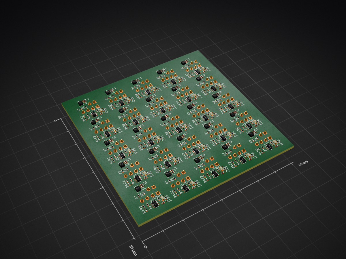
TrackNodeAccel panel is an open-source printed circuit board by Project-Touchscape, from the Project-Touchscape/Touchscape-PCB repository on GitHub. It is a 2-layer board of 81 × 81 mm with 375 parts on 275 nets, routed with 1,925 tracks and 200 vias.
It is built around the TLV493D-A1B6 and LIS2DTW12. Its parts include 175 resistors, 75 capacitors, 50 ICs, 50 connectors and 25 diodes.
| Qty | Value | Footprint | References |
|---|---|---|---|
| 100 | 100 | Resistor_SMD:R_0402_1005Metric | R1, R1, R1, R1, R1, R1, R1, R1, R1, R1, R1, R1, R1, R1, R1, R1 +84 |
| 75 | 0.1uF | Capacitor_SMD:C_0402_1005Metric | C1, C1, C1, C1, C1, C1, C1, C1, C1, C1, C1, C1, C1, C1, C1, C1 +59 |
| 50 | 1.2K | Resistor_SMD:R_0402_1005Metric | R3, R3, R3, R3, R3, R3, R3, R3, R3, R3, R3, R3, R3, R3, R3, R3 +34 |
| 25 | 500 | Resistor_SMD:R_0402_1005Metric | R5, R5, R5, R5, R5, R5, R5, R5, R5, R5, R5, R5, R5, R5, R5, R5 +9 |
| 25 | Conn_01x02 | Connector_PinHeader_2.54mm:PinHeader_1x02_P2.54mm_Vertical | J2, J2, J2, J2, J2, J2, J2, J2, J2, J2, J2, J2, J2, J2, J2, J2 +9 |
| 25 | Conn_01x04 | Connector_PinHeader_2.54mm:PinHeader_1x04_P2.54mm_Vertical | J1, J1, J1, J1, J1, J1, J1, J1, J1, J1, J1, J1, J1, J1, J1, J1 +9 |
| 25 | LED | LED_SMD:LED_0603_1608Metric | D1, D1, D1, D1, D1, D1, D1, D1, D1, D1, D1, D1, D1, D1, D1, D1 +9 |
| 25 | LIS2DTW12 | Package_LGA:LGA-12_2x2mm_P0.5mm | U2, U2, U2, U2, U2, U2, U2, U2, U2, U2, U2, U2, U2, U2, U2, U2 +9 |
| 25 | TLV493D-A1B6 | Package_SO:TSOP-6_1.65x3.05mm_P0.95mm | U1, U1, U1, U1, U1, U1, U1, U1, U1, U1, U1, U1, U1, U1, U1, U1 +9 |
It measures 81 × 81 mm and has 2 copper layers, 1.6 mm thick.
375 parts, built around the TLV493D-A1B6 and LIS2DTW12. The full list of its parts is on this page, with links to each part's symbol and footprint where PCBKit's library has them.
From the Project-Touchscape/Touchscape-PCB repository on GitHub, at the commit this page was made from: the board is TrackNodeAccel/TrackNodeAccel-panel.kicad_pcb and its schematic AS5600_Mockup/AS5600_Mockup.kicad_sch. PCBKit opens the board in the browser, with nothing to install.
Its repository states no licence, so its author keeps all rights: ask Project-Touchscape before reusing the design.
Project-Touchscape/Touchscape-PCB
PCB designs for sensors, drivers, routing, and communication

Project-Touchscape/Touchscape-PCB
PCB designs for sensors, drivers, routing, and communication

Project-Touchscape/Touchscape-PCB
PCB designs for sensors, drivers, routing, and communication

Project-Touchscape/Touchscape-PCB
PCB designs for sensors, drivers, routing, and communication

Project-Touchscape/Touchscape-PCB
PCB designs for sensors, drivers, routing, and communication

Project-Touchscape/Touchscape-PCB
PCB designs for sensors, drivers, routing, and communication

Project-Touchscape/Touchscape-PCB
PCB designs for sensors, drivers, routing, and communication

Project-Touchscape/Touchscape-PCB
PCB designs for sensors, drivers, routing, and communication

Project-Touchscape/Touchscape-PCB
PCB designs for sensors, drivers, routing, and communication

Project-Touchscape/Touchscape-PCB
PCB designs for sensors, drivers, routing, and communication

swanmatch/MxLEDBitPCB
プロジェクト | スイッチ | Kailhソケット利用可否 | LED | スルーホールダイオード | SOD-123 | -|-|-|-|-|- Nexus | MX | No | SK6812MINI | Yes | No | Altana | MX | Yes | SK6812MINI | Yes | No | Suxen | MX | No | YS-SK6812MINI | Yes | Yes() | Container |…

linux-automation/candleLightFD
USB CAN-FD interface based on the STM32G0 that works well with gs_usb on Linux


climent/Sarcodina
Sarcodina is an implementation of MxLEDBit with horizontal power distribution.

Envious-Data/EnvOpenEnvSensor
a simple sensor pcb with a display to show some environment conditions

gohanda11/Split60HE
Split60HE is a split (left/right) version of the 60% Hall-effect keyboard HE60, designed in KiCad.


reven/V6-conversion
Hardware and firmware to convert a V6 Keychron keyboard to north-facing LEDs.