

2 layers81 × 81 mm
TrackNodeAccel panel
Project-Touchscape/Touchscape-PCB
PCB designs for sensors, drivers, routing, and communication
375 parts
 Project-Touchscape/Touchscape-PCB
PCB designs for sensors, drivers, routing, and communication
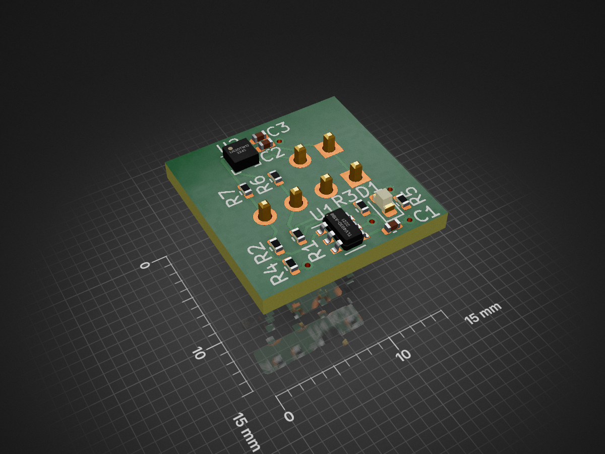
TrackNodeAccel is an open-source printed circuit board by Project-Touchscape, from the Project-Touchscape/Touchscape-PCB repository on GitHub. It is a 2-layer board of 15 × 15 mm with 15 parts on 11 nets, routed with 77 tracks and 8 vias.
It is built around the TLV493D-A1B6 and LIS2DTW12. Its parts include 7 resistors, 3 capacitors, 2 ICs, 2 connectors and 1 diode.
| Qty | Value | Footprint | References |
|---|---|---|---|
| 4 | 100 | Resistor_SMD:R_0402_1005Metric | R1, R2, R6, R7 |
| 3 | 0.1uF | Capacitor_SMD:C_0402_1005Metric | C1, C2, C3 |
| 2 | 1.2K | Resistor_SMD:R_0402_1005Metric | R3, R4 |
| 1 | 500 | Resistor_SMD:R_0402_1005Metric | R5 |
| 1 | Conn_01x02 | Connector_PinHeader_2.54mm:PinHeader_1x02_P2.54mm_Vertical | J2 |
| 1 | Conn_01x04 | Connector_PinHeader_2.54mm:PinHeader_1x04_P2.54mm_Vertical | J1 |
| 1 | LED | LED_SMD:LED_0603_1608Metric | D1 |
| 1 | LIS2DTW12 | Package_LGA:LGA-12_2x2mm_P0.5mm | U2 |
| 1 | TLV493D-A1B6 | Package_SO:TSOP-6_1.65x3.05mm_P0.95mm | U1 |
It measures 15 × 15 mm and has 2 copper layers, 1.6 mm thick.
15 parts, built around the TLV493D-A1B6 and LIS2DTW12. The full list of its parts is on this page, with links to each part's symbol and footprint where PCBKit's library has them.
From the Project-Touchscape/Touchscape-PCB repository on GitHub, at the commit this page was made from: the board is TrackNodeAccel/TrackNodeAccel.kicad_pcb and its schematic AS5600_Mockup/AS5600_Mockup.kicad_sch. PCBKit opens the board in the browser, with nothing to install.
Its repository states no licence, so its author keeps all rights: ask Project-Touchscape before reusing the design.
Project-Touchscape/Touchscape-PCB
PCB designs for sensors, drivers, routing, and communication

Project-Touchscape/Touchscape-PCB
PCB designs for sensors, drivers, routing, and communication

Project-Touchscape/Touchscape-PCB
PCB designs for sensors, drivers, routing, and communication

Project-Touchscape/Touchscape-PCB
PCB designs for sensors, drivers, routing, and communication

Project-Touchscape/Touchscape-PCB
PCB designs for sensors, drivers, routing, and communication

Project-Touchscape/Touchscape-PCB
PCB designs for sensors, drivers, routing, and communication

Project-Touchscape/Touchscape-PCB
PCB designs for sensors, drivers, routing, and communication

Project-Touchscape/Touchscape-PCB
PCB designs for sensors, drivers, routing, and communication

Project-Touchscape/Touchscape-PCB
PCB designs for sensors, drivers, routing, and communication

Project-Touchscape/Touchscape-PCB
PCB designs for sensors, drivers, routing, and communication

google/mozc-devices
Circuit diagrams and firmware source code for Gboard DIY keyboards

hoglet67/RGBtoHDMI
Bare-metal Raspberry Pi project that provides pixel-perfect sampling of Retro Computer RGB/YUV video and conversion to HDMI

mntmn/amiga2000-gfxcard
MNT VA2000, an Open Source Amiga 2/3/4000 Graphics Card (Zorro II/III), written in Verilog

hackclub/OnBoard
💡 Join 1,000 teenagers and make your first PCB with a $100 grant!

kenp-io/not-for-airpods-repairs
The content of this repository is licensed under the WTFPL License. Please have a close look at the terms before using this material.

Luos-io/luos_engine
Open-source and real-time orchestrator for cyber-physical-systems, to easily design, test and deploy embedded applications and digital twins.

Chrismettal/EleLab_v2
Cheap DIY lab system for hobbyists and the tinkering folk
