
4 layers99 × 53.3 mm
PSLab
fossasia/pslab-hardware
PSLab Hardware Design and Schematics https://pslab.io
199 parts1.7kApache-2.0

 pohjolaworks/Sotka12
Split mechanical keyboard with orthogonal layout and detachable extra row
Sotka is an open-source printed circuit board by pohjolaworks, from the pohjolaworks/Sotka repository on GitHub, published under the MIT licence. It is a 2-layer board of 133.1 × 117.4 mm with 74 parts on 60 nets, routed with 678 tracks and 0 vias.
It is built around the WS2812B. Its parts include 31 diodes, 31 switches, 4 connectors and 1 IC. It belongs with the keyboards and input boards and the AVR (ATmega, ATtiny) boards of this library.
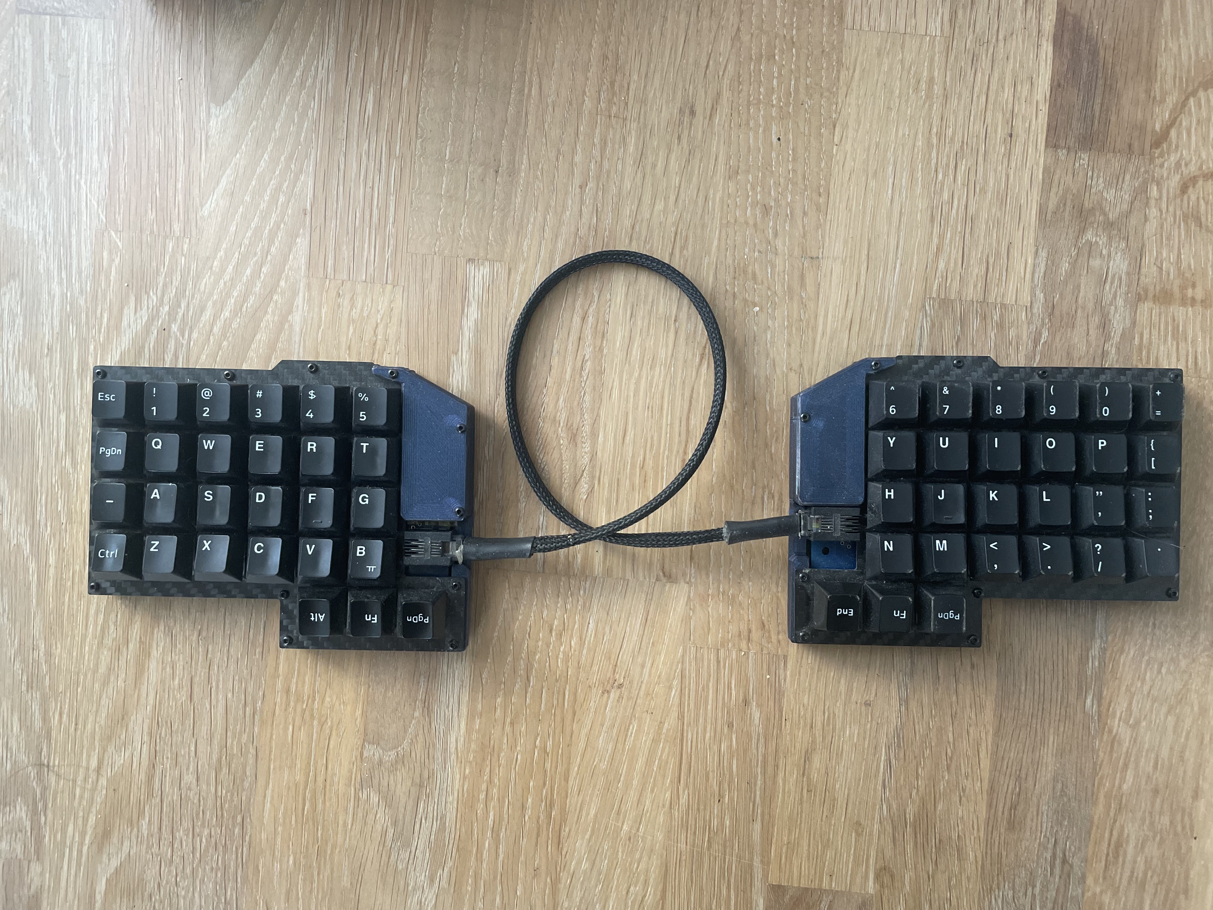
Split mechanical keyboard with orthogonal layout and detachable extra row
Uses an RJ12 cable for serial communication between the halves.
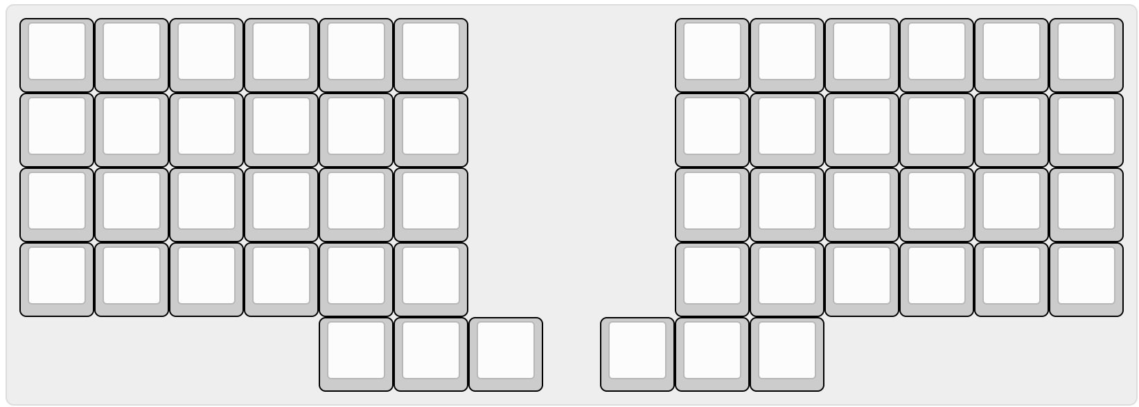
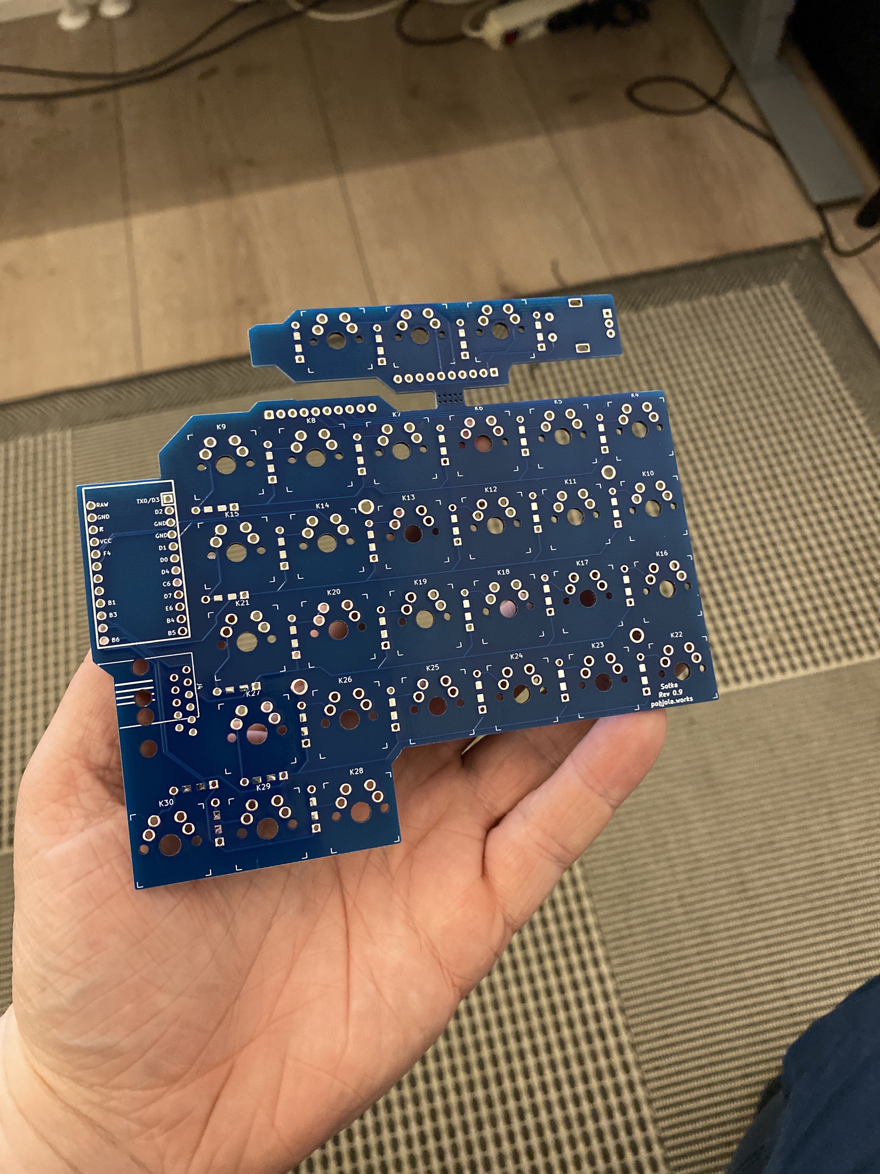
| Qty | Value | Footprint | References |
|---|---|---|---|
| 31 | D | Keebio-Parts:Diode-dual | D2, D10, D11, D12, D13, D14, D15, D16, D17, D18, D19, D20, D21, D22, D23, D24 +15 |
| 30 | KEYSW | keyswitches:SW_MX_reversible | K1, K2, K10, K11, K12, K13, K14, K15, K16, K17, K18, K19, K20, K21, K22, K23 +14 |
| 4 | MountingHole_4mm | keyboard_parts:MountingHole_M2 | HOLE5, HOLE5, HOLE5, HOLE5 |
| 2 | 6P6C | pretty_footprints:RJ11-MOLEX | J3, J4 |
| 2 | Conn_01x10 | Connector_JST:JST_EH_B10B-EH-A_1x10_P2.50mm_Vertical | J1, J2 |
| 1 | ProMicro | Keebio-Parts:ArduinoProMicro | U1 |
| 1 | Rotary_Encoder_Switch | Keebio-Parts:RotaryEncoder_Alps_EC11E-Switch_Vertical_H20mm | SW1 |
| 1 | WS2812B | LED_SMD:LED_WS2812B_PLCC4_5.0x5.0mm_P3.2mm | RGB1 |
The 72 most common of 74 parts.
fossasia/pslab-hardware
PSLab Hardware Design and Schematics https://pslab.io

FrameworkComputer/ExpansionCards
Reference designs and documentation to create Expansion Cards for the Framework Laptop


PrintersForAnts/Micron
If you want to purchase full kits there are 3 available (Kits are slowly updating to R1 hardware just make sure to double check the included hardware in your kit and if you have any questions reach out in the discord)


It measures 133.1 × 117.4 mm and has 2 copper layers, 1.6 mm thick.
74 parts, built around the WS2812B. The full list of its parts is on this page, with links to each part's symbol and footprint where PCBKit's library has them.
From the pohjolaworks/Sotka repository on GitHub, at the commit this page was made from: the board is Sotka.kicad_pcb. PCBKit opens the board in the browser, with nothing to install.
Its repository publishes it under the MIT licence: you may reuse it on that licence's terms (keep the author's notice, and for a copyleft licence share your changes alike).