2 layers50 × 70 mm

 pjontop/pjboard-prod
PJBoard is a low-profile, wireless split keyboard with 42 keys, two displays, and a very very thin case!
Pjboardv2 is an open-source printed circuit board by pjontop, from the pjontop/pjboard-prod repository on GitHub. It is a 2-layer board of 261.5 × 83 mm with 113 parts on 95 nets, routed with 477 tracks and 61 vias.
It is built around the SSSS811101 and TS-1114S-26. Its parts include 46 switches, 42 diodes and 2 ICs. It belongs with the nRF52 and nRF5x boards of this library.


PJBoard is a low-profile, wireless split keyboard with 42 keys, two displays, and a very very thin case!
I made this because I wanted something that had the clean look of keyboards like the Geist Totem and the portability of the Voyager, but with a few more keys so it would be easier for me to actually learn how to use a split keyboard. Basically: how close can I get to the MacBook Pro of keyboards?
It uses Kailh Choc switches, two SuperMini nRF52840 controllers, nice!view displays, and ZMK firmware. Each half is completely wireless and has its own battery, power switch, and reset button.
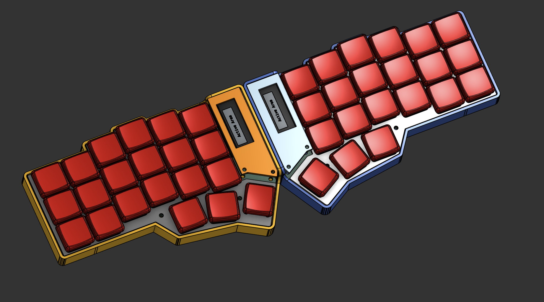
The case was made in Onshape. I started by importing the PCB outline and building everything around it, which sounds simple until Onshape decides one switch model needs approximately one billion triangles and takes four hours to import :sob:
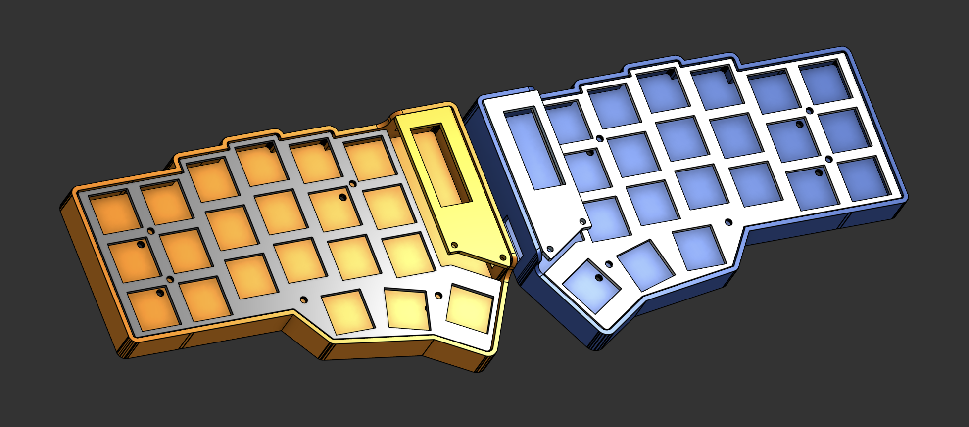
The final case is made from three parts per side: the base, the switch plate, and the display cover. I wanted it to be really thin, rounded, and clean, so the mounting hardware is hidden and the top pieces sit flush with the case. There are also cutouts underneath the larger components so the case does not need to be unnecessarily chonky.
You can view and remix the original CAD here: PJBoard on Onshape
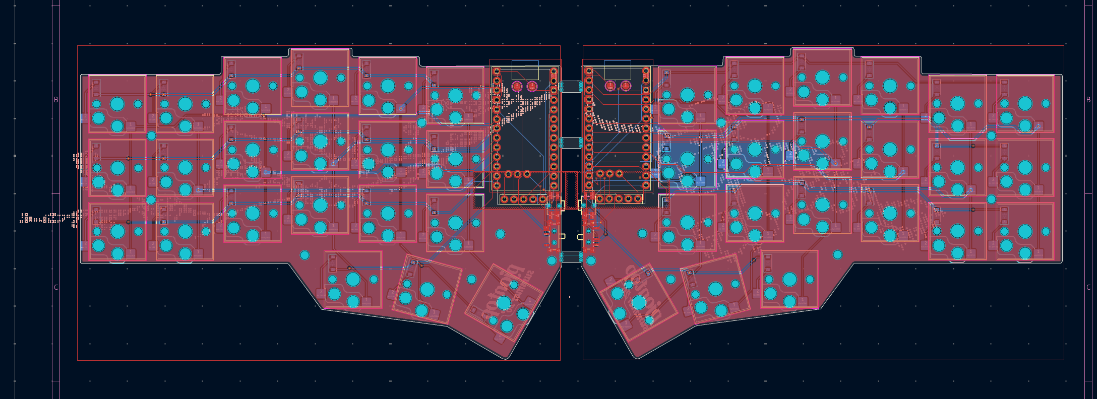
Here is the PCB! It was designed in KiCad and it was definitely the largest rabbit hole in this entire project.
Each half uses a 4x6 key matrix with 21 populated positions, one diode per key, a SuperMini nRF52840, a nice!view header, an on/off switch, and a reset button. I moved the diodes into the centre control area to keep the switch area clean and used both copper layers to make the matrix routing actually possible.
The two halves are panelized together with breakaway tabs, so they can be manufactured as one PCB and snapped apart afterward. Fire, right?
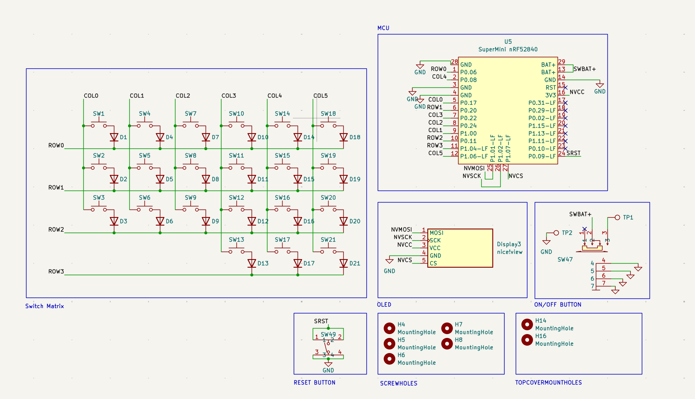
PJBoard runs ZMK since the keyboard is wireless. Prebuilt firmware for both halves is included in the firmware folder, along with the source configuration.
The current keymap has three layers:
The two thumb layer keys make it possible to keep the board at only 42 keys without losing all the useful stuff. The displays stay visible while the keyboard is awake and show the current keyboard status.
Here should be the main stuff you need to build PJBoard:
A better BOM Can be found in the bom.csv in the main directory, this is merely meant for a rough look over.
This was my first time going this deep into designing a keyboard, and I learnt a TON.
KiCad was the main villain here. I redesigned the PCB more than once, moved all the diodes around, fought with mirrored layouts, installed a plugin that did not even do what I needed, and eventually figured out a routing setup that was way cleaner. Sad reality: sometimes you really do just have to reroute the entire board.
The case also took a bunch of iteration. I wanted it thin, rounded, strong around the high-pressure keys, and completely clean from the top with no visible screws. Getting all of those things at once was much harder than sketching them, especially while keeping enough room for the hotswap sockets, batteries, controllers, and displays.
The firmware was another whole thing. ZMK is really powerful, but understanding boards vs shields, setting up both halves, fixing the matrix, and getting the displays working was WAY worse than I thought it would be. YouTube tutorials, random websites, and an unreasonable amount of debugging carried me through it.
Overall, though, I am super happy with how it turned out. I went from a rough idea and a hand sketch to a complete PCB, case, and working firmware setup. Very very fire.
I am super thankful to Hack Club for funding this project and making it possible for me to actually build the weird keyboard I spent way too many hours obsessing over.
Also, Macondo is awesome. Seriously. Programs like this are the reason I can learn hardware by actually making something real instead of just watching another tutorial and forgetting everything five minutes later.
alr toodles :3
| Qty | Value | Footprint | References |
|---|---|---|---|
| 42 | D | Diode_SMD:D_SOD-123 | D1, D2, D10, D11, D12, D13, D14, D15, D16, D17, D18, D19, D20, D21, D22, D23 +26 |
| 42 | SW_Push | keyboard_models:SW_Hotswap_Kailh_Choc_V1_Assembly | SW1, SW2, SW10, SW11, SW12, SW13, SW14, SW15, SW16, SW17, SW18, SW19, SW20, SW21, SW24, SW25 +26 |
| 14 | MountingHole | pjboard:MountingHole_M2_NPTH | H4, H5, H6, H7, H8, H9, H10, H11, H12, H13, H14, H15, H16, H17 |
| 4 | TestPoint | TestPoint:TestPoint_Pad_D2.0mm | TP1, TP2, TP3, TP4 |
| 3 | MountingHole | pjboard:BreakawayTab | H1, H2, H3 |
| 2 | SSSS811101 | lcsc_keyboard:SW-SMD_SSSS811101 | SW47, SW48 |
| 2 | SuperMini nRF52840 | PCM_marbastlib-xp-promicroish:SuperMini_nRF52840_AH_USBup | U5, U6 |
| 2 | TS-1114S-26 | lcsc_keyboard:SW-SMD_4P-L4.7-W4.5-P1.70-LS6.4-EH | SW49, SW50 |
| 2 | nice!view | nv:nice_view | Display3, Display4 |


h0lad/SolarMeshtasticNode
This is a Meshtastic Solar Node PCB based on the Heltec HT-CT62 and the linear solar charge controller TI BQ25185.

ZigEmbeddedGroup/sycl-badge
The badge for the SYCL conference! https://zigembeddedgroup.github.io/sycl-badge/


chrisg20/CarThingBridge
A compact connector board for the Spotify Car Thing and Raspberry Pi Zero.


h0lad/LoRaHarvesterBox
PCB integrating a ST STM32WLE5CC and TI BQ25570 energy harvester. Ideal platform for ultra-low-power LoRa(WAN) nodes projects.
It measures 261.5 × 83 mm and has 2 copper layers, 1.6 mm thick.
113 parts, built around the SSSS811101 and TS-1114S-26. The full list of its parts is on this page, with links to each part's symbol and footprint where PCBKit's library has them.
From the pjontop/pjboard-prod repository on GitHub, at the commit this page was made from: the board is pcb/pjboardv2.kicad_pcb and its schematic pcb/pjboardv2.kicad_sch. PCBKit opens the board in the browser, with nothing to install.
Its repository states no licence, so its author keeps all rights: ask pjontop before reusing the design.