
4 layers100 × 123 mm
Duet2
Duet3D/Duet-2-Hardware
The KiCAD source for the Duet 3d printer controller see www.duet3d.com
356 parts258

 mrnuke/beaglebone-spi-flasher-cape3
The SPI flasher cape is a cape for the BeagleBone family of boards which allows the BeagleBone to interface with a SPI NOR flash chip in order to allow programming or reading the chip's contents.
Beagleflash is an open-source printed circuit board by mrnuke, from the mrnuke/beaglebone-spi-flasher-cape repository on GitHub. It is a 2-layer board of 86.4 × 54.6 mm with 23 parts on 105 nets, routed with 407 tracks and 49 vias.
It is built around the 74HC125D. Its parts include 9 connectors, 4 capacitors, 3 resistors, 3 ICs and 1 switch.
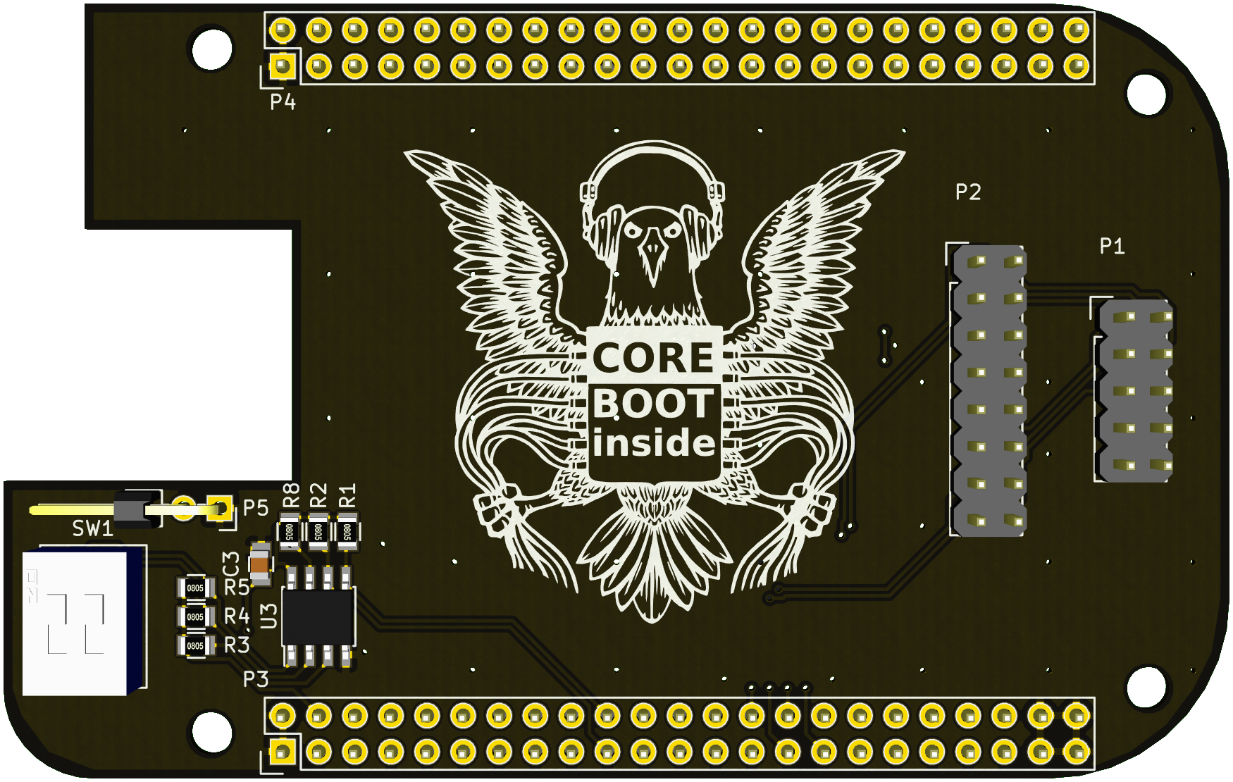
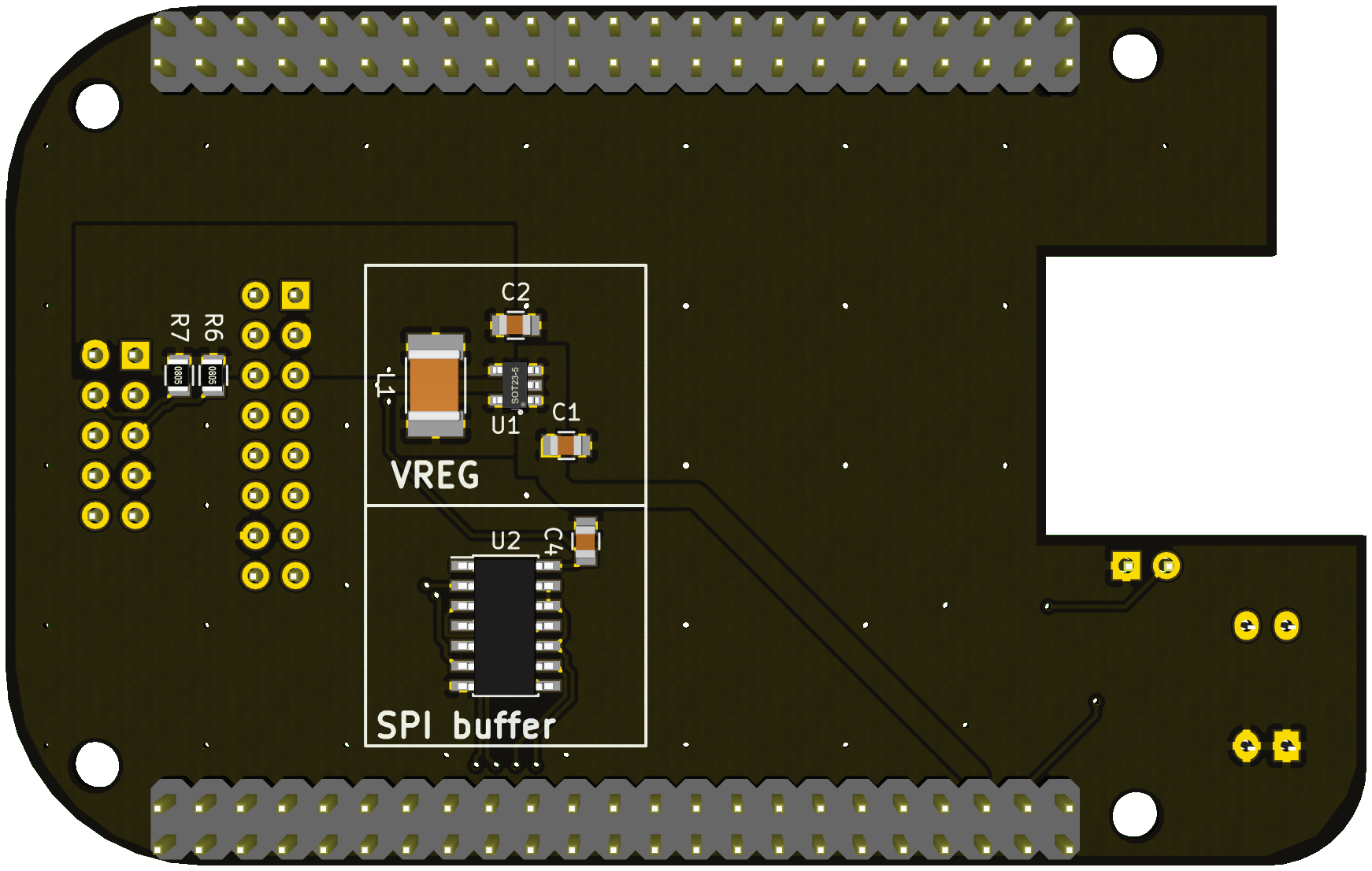
The SPI flasher cape is a cape for the BeagleBone family of boards which allows the BeagleBone to interface with a SPI NOR flash chip in order to allow programming or reading the chip's contents.
The total bill-of-materials (COM) cost is under $10 US, including the PCB.
The independent voltage regulator (VR) supplies the power for the operation of the SPI chip, and is independent of te BeagleBone's internal voltage rails. This protects the BeagleBone from brown-outs inc case of an external short-circuits. Since it is a switching regulator, the VR dissipates very little power when compared to more common linear regulators.
The SPI buffer IC protects the internal pins of the BeagleBone from ESD and short-circuits. The buffer IC is powered from the independent VR, and prevents excessive currents from being sourced by the BeagleBone's processor in case of short-circuits.
The buffer IC is driven by the CS signal of the SPI interface, which means that the outputs are high-impedance when no SPI communication is taking place. As a result, the SPI chip does not have to be disconnected when the target system is powered on. Also, since the buffer is enabled by the CS signal, there is no extra software configuration that needs to be done before enabling the signal path to the SPI chip, as there is on other solutions (e.g. Gogole servo board). It's all automatic!
The integrated EEPROM informs the BeagleBone what pins are used by the cape, so the cape is automatically detected, and the interfaces pins are automatically configured.
The external pin headers match the pinout of 8-pin and 16-pin SPI flash parts so that programming clips (e.g. Pomona SOIC-8) may be directly connected to the cape.
The integrated pull-up resistors ensure that the HOLD and WP lines of the SPI chip are driven appropriately. This allows "naked" chips to be programmed. For mounted SPI chips, the pull-ups prevent short-circuits if another component on the target system drives these signals low.
This folder contains the KiCad schematic and board files
3D renderings of the PCB.
| Qty | Value | Footprint | References |
|---|---|---|---|
| 4 | CONN_01X01 | Mounting_Holes:MountingHole_3.2mm_M3_ISO14580_Pad | P6, P7, P8, P9 |
| 3 | 10k | Resistors_SMD:R_0805 | R1, R2, R3 |
| 3 | 10uF | Capacitors_SMD:C_0805 | C1, C2, C3 |
| 1 | 0.1uF | Capacitors_SMD:C_0805 | C4 |
| 1 | 10k | Housings_SOIC:SOIC-16_3.9x9.9mm_Pitch1.27mm | RP1 |
| 1 | 10uH | Inductors_NEOSID:Neosid_Inductor_SM-NE45_SMD1812 | L1 |
| 1 | 74HC125 | Housings_SOIC:SOIC-14_3.9x8.7mm_Pitch1.27mm | U2 |
| 1 | BBB_P8 | Pin_Headers:Pin_Header_Straight_2x23 | P5 |
| 1 | BBB_P9 | Pin_Headers:Pin_Header_Straight_2x23 | P4 |
| 1 | CAT24C256W | Housings_SOIC:SOIC-8_3.9x4.9mm_Pitch1.27mm | U3 |
| 1 | DIPS_02 | Buttons_Switches_ThroughHole:SW_DIP_x2_Slide | SW1 |
| 1 | EEPROM_PROG_EN | Pin_Headers:Pin_Header_Angled_2x01 | P3 |
| 1 | LOGO | logo-coreboot | G*** |
| 1 | PAM2305AAB330 | TO_SOT_Packages_SMD:SOT-23-5 | U1 |
| 1 | SPI-16 | Connect:IDC_Header_Straight_16pins | P2 |
| 1 | SPI-8 | Connect:IDC_Header_Straight_10pins | P1 |
Duet3D/Duet-2-Hardware
The KiCAD source for the Duet 3d printer controller see www.duet3d.com


cester-ino/OTTO-hardware
those specs refer to the tactile buttons version, but a led backlight button version is in the works too.

idlehandsdev/pps-watch
An extremely accurate watch that doesn't tell time.

46nori/Z80Atmega128
Real Z80A system with I/O emulated by AVR(ATmega128)


ArtoLabs/Sensi-pot
Collection of modules for indoor/outdoor gardening automation and environmental control

It measures 86.4 × 54.6 mm and has 2 copper layers, 1.6 mm thick.
23 parts, built around the 74HC125D. The full list of its parts is on this page, with links to each part's symbol and footprint where PCBKit's library has them.
From the mrnuke/beaglebone-spi-flasher-cape repository on GitHub, at the commit this page was made from: the board is kicad/beagleflash.kicad_pcb. PCBKit opens the board in the browser, with nothing to install.
Its repository states no licence, so its author keeps all rights: ask mrnuke before reusing the design.