4 layers97.4 × 94.7 mm
ReClockator-500
mrehkopf/ReClockator-500
Changes the orientation of a 68000 DIP CPU, adds 4 clock ports
20 parts2GPL-3.0

 mrehkopf/Ginger12
Socket shift, CPU switch, Clockports for Amiga mITX "Denise"
Ginger is an open-source printed circuit board by mrehkopf, from the mrehkopf/Ginger repository on GitHub. It is a 4-layer board of 65.4 × 111.6 mm with 30 parts on 102 nets, routed with 1,040 tracks and 96 vias.
It is built around the 74HCT245, 74HCT4053D and 74HCT08D, with the 74HCT139D and 74HCT688D among its other parts. Its parts include 9 capacitors, 9 ICs, 5 connectors and 4 resistors. It belongs with the retro computing and games boards of this library.


Ginger is an integrated Socket Shift, 2x CPU switch, and 4x Clock Port & RTC expansion, for use with the A500+ mITX ("Denise") board by Enterlogic.
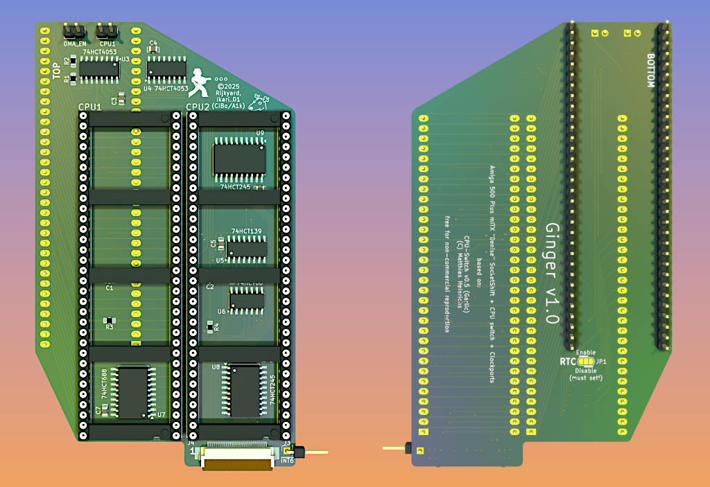
Enables simultaneous use of accelerator boards and the Denise CF-Floppy I/O PCB.
The socket shift is designed primarily to accomodate Matthias Heinrichs' accelerators 68EC020-TK (in CPU1 socket) or 68030-TK2 (in CPU2 socket), although others will probably work as long as they are not unreasonably large.
Keep both your accelerator and OG 68000 CPU available easily with the flick of a switch!
This allows the 68000 CPU, when enabled, to make use of DMA resources - like an IDE controller - that reside on the accelerator board.
This feature is tested with recent firmwares of the 68EC020-TK and 68030-TK2 by Matthias Heinrichs.
It might not work with other accelerator boards. The function is accomplished by connecting the RESET signal of the active CPU to the (otherwise inactive) accelerator board instead of constantly holding the accelerator's RESET line low all the time.
Four clock ports (in the sense of Gayle's "SPARE" mapping) and one RTC port (for actual clock use) are made available on the 30-pin FPC connector.
In order to plug in the Ginger into the Denise's CPU socket the pins should have a length of about 8.5mm between the Ginger PCB and the Denise's CPU socket. Otherwise the Ginger or any plugged-in accelerators will collide with other parts on the Denise board.
A viable part is Mill-Max 342-10-164-00-592000 which can be cut in half to yield two rows of 32 pins each.
Alternatively it is possible to stack multiple DIP64 sockets to reach the desired height.
Four buffered clock ports (with a single shared RTC mapping) are available on the 30-lead FPC connector.
The four clock ports (represented by the /SPAREn_CS signals) are mapped as follows:
$D80001$D84001$D88001$D8C001Adapter PCBs with actual clock port pin headers are available:
Repository: ClockPort-FPC-Adapters
The Adapter PCBs have non-mirrored pinouts on their respective FPC connectors, so a "B-Type" FPC cable has to be used, where the contact surfaces at the ends are on opposite sides (top ↔ bottom).
The FPC pinout is as follows:
| Pin # | Function |
|---|---|
| 1 | GND |
| 2 | +5V |
| 3 | +5V |
| 4 | +5V |
| 5 | /INT6 |
| 6 | /SPARE0_CS |
| 7 | /SPARE1_CS |
| 8 | /SPARE2_CS |
| 9 | /SPARE3_CS |
| 10 | GND |
| 11 | /RTC_CS |
| 12 | /RTC_PWRBAD |
| 13 | /IORD |
| 14 | /IOWR |
| 15 | A5 |
| 16 | A4 |
| 17 | GND |
| 18 | A3 |
| 19 | A2 |
| 20 | D23 |
| 21 | D22 |
| 22 | D21 |
| 23 | GND |
| 24 | D20 |
| 25 | D19 |
| 26 | D18 |
| 27 | D17 |
| 28 | D16 |
| 29 | /RESET |
| 30 | GND |
An additional /INT6 pin is present next to the FPC connector. This pin must be connected to the /INT6 signal on the Amiga's main board e.g. using a jumper wire since it is not available on the CPU socket.
The Denise provides a pin header containing the signal.
Do NOT leave this jumper open! This jumper must be soldered in the "Enable" or "Disable" position! If left open, RTC and/or clock ports will be unreliable.
You must solder this jumper in the "Disabled" position when another RTC expansion is used anywhere on the computer.
$DC0001 is enabled.$DC0001 is disabled.| Reference | Part # | Package | Qty. |
|---|---|---|---|
| C1..C9 | 100nF ≥16V X5R | SMT 0805 | 9 |
| R1..R4 | 10kΩ 0.1W | SMT 0805 | 4 |
| U1, U2 | DIP64 socket | THT, 2.54mm pitch, 22.86mm row spacing | 2 |
| U3, U4 | 74HCT4053 | SOIC-16 | 2 |
| U5 | 74HCT139 | SOIC-16 | 1 |
| U6 | 74HCT08 | SOIC-8 | 1 |
| U7 | 74HCT688 | SOIC-20 | 1 |
| U8, U9 | 74HCT245 | SOIC-20 | 2 |
| J1, J2 | 2x1 Pin Header | THT 2.54mm | 2 |
| J3 | 1x1 Pin Header | THT 2.54mm 90° | 1 |
| J4 | https://aliexpress.com/item/1005003981823532.html TE 3-1734592-0 Molex 524373071 Amphenol F32R-1A7H1-11030 | 30-lead FPC connector SMT 0.5mm pitch | 1 |
| P1 | 1x Mill-Max 342-10-164-00-592000 2x Samtec BBS-132-T-B 2x Samtec BBS-132-G-B | 1x32 8.51mm machined post connectors | 1 / 2 |
| P1 (alt.) | DIP64 sockets (stacked) | THT, 2.54mm pitch, 22.86mm row spacing | ~2 |
Based on prior work by Matthias Heinrichs (CPU switch "Garlic") and Rijkyard (socket shift).
Free for non-commercial use as per prior work's license.
| Qty | Value | Footprint | References |
|---|---|---|---|
| 9 | 100n | Capacitor_SMD:C_0805_2012Metric_Pad1.18x1.45mm_HandSolder | C1, C2, C3, C4, C5, C6, C7, C8, C9 |
| 4 | 10k | Resistor_SMD:R_0805_2012Metric_Pad1.20x1.40mm_HandSolder | R1, R2, R3, R4 |
| 2 | 74HCT245 | Package_SO:SOIC-20W_7.5x12.8mm_P1.27mm | U8, U9 |
| 2 | 74HCT4053 | Package_SO:SOIC-16_3.9x9.9mm_P1.27mm | U3, U4 |
| 1 | 74HCT08 | Package_SO:SOIC-14_3.9x8.7mm_P1.27mm | U6 |
| 1 | 74HCT139 | Package_SO:SOIC-16_3.9x9.9mm_P1.27mm | U5 |
| 1 | 74HCT688 | Package_SO:SOIC-20W_7.5x12.8mm_P1.27mm | U7 |
| 1 | CPU1 | Package_DIP:DIP-64_W22.86mm_Socket_LongPads | U1 |
| 1 | CPU1_EN | Connector_PinHeader_2.54mm:PinHeader_1x02_P2.54mm_Vertical | J1 |
| 1 | CPU2 | mypackages:DIP-64_W22.86mm_Socket_LongPads_machinedsocket3dmodel | U2 |
| 1 | Conn_01x01_Pin | Connector_PinHeader_2.54mm:PinHeader_1x01_P2.54mm_Horizontal | J3 |
| 1 | Conn_01x30 | mypackages:FPC_30pin_0.5mm_average | J4 |
| 1 | DMA_EN | Connector_PinHeader_2.54mm:PinHeader_1x02_P2.54mm_Vertical | J2 |
| 1 | LOGO | LOGO | G*** |
| 1 | LOGO | rehkopf:LOGO_6.5x4.8 | G*** |
| 1 | Mainboard | Package_DIP:DIP-64_W22.86mm_Socket_LongPads | P1 |
| 1 | RTC_Enable | Jumper:SolderJumper-3_P1.3mm_Open_RoundedPad1.0x1.5mm | JP1 |
It measures 65.4 × 111.6 mm and has 4 copper layers, 1.6 mm thick.
30 parts, built around the 74HCT245, 74HCT4053D, 74HCT08D and 74HCT139D. The full list of its parts is on this page, with links to each part's symbol and footprint where PCBKit's library has them.
From the mrehkopf/Ginger repository on GitHub, at the commit this page was made from: the board is Ginger.kicad_pcb and its schematic Ginger.kicad_sch. PCBKit opens the board in the browser, with nothing to install.
Its repository states no licence, so its author keeps all rights: ask mrehkopf before reusing the design.
mrehkopf/ReClockator-500
Changes the orientation of a 68000 DIP CPU, adds 4 clock ports


Julesc013/project-carbon
Hardware and software for custom CPUs, FPUs, and computer systems.